|
|
|
PDF TS32101 Data sheet ( Hoja de datos )
| Número de pieza | TS32101 | |
| Descripción | High Efficiency DC/DC Boost Converter | |
| Fabricantes | Semtech | |
| Logotipo | ||
Hay una vista previa y un enlace de descarga de TS32101 (archivo pdf) en la parte inferior de esta página. Total 12 Páginas | ||
|
No Preview Available !
TRIUNE PRODUCTS
Features
• Output up to 1.5A at 5.0V with 1.8V input
• Wide input voltage range: 1.75V – 5.5V
• Output current up to 2A
• Robust operation during hot-load disconnect and hot-
load disable
• Adjustable output voltage up to 5.5V
• Adjustable output current limit
• Includes full output isolation/reverse current blocking
when disabled
• 2 MHz ± 10% fixed switching frequency
• Low power mode
• High efficiency – up to 95%
• Full protection for over-current, over-temperature, VOUT
over-voltage, and VIN under-voltage
• Power good/fault indication
Summary Specifications
• Ambient operating temperature -40C to 85C
• Packaged in a 16pin QFN (3x3)
TS32101
High Efficiency DC/DC
Boost Converter for USB, 2Mhz
Description
The TS32101 is a DC/DC synchronous switching Boost
Converter with fully integrated power switches, internal PWM
current mode compensation, and full fault protection. The
switching frequency of 2 MHz was chosen to enable the use
of small external components for portable applications. The
device also has a constant output current limit loop to provide
a sharp output current limit that doesn’t move significantly
with input voltage and output voltage.
Applications
• USB power
• Portable products
• Wireless remote sensors
• Emergency chargers
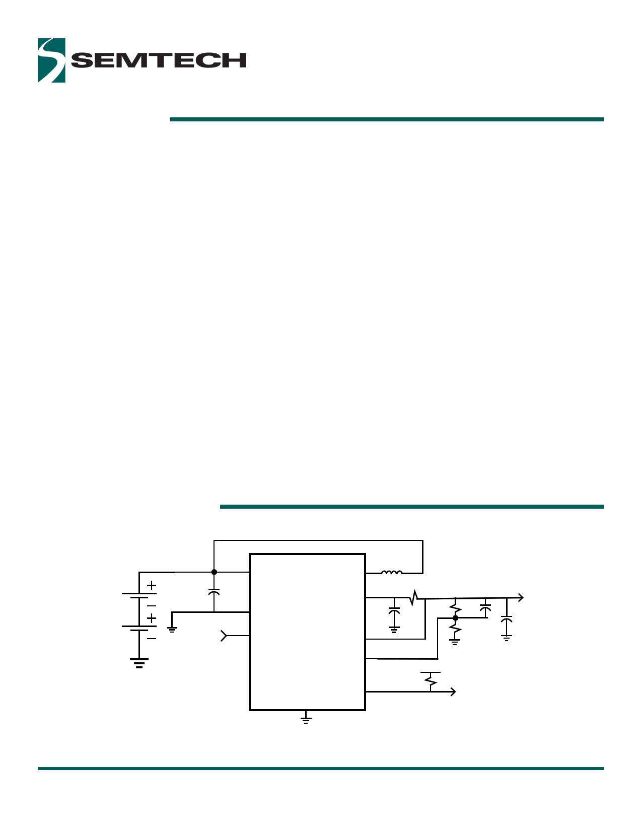
Typical Application Circuit
VIN VSW
TS32101
CIN ISEN
GND
LOUT
1 uH
RSENSE
COUT
2 x 22 uF
EN VOUT
RTOP
RBOT
VOUT2
CFF
COUT2
PGND
FB
PG
VDD
RPULLUP
(optional)
TS32101
Final Datasheet
January 26, 2016
Rev 2.1
www.semtech.com
1 of 12
Semtech
1 page 
Characteristics
Electrical Characteristics, TA = -40C to 85C, VIN =2.4V (unless otherwise noted)
Symbol
Parameter
Condition
Min Typ Max Unit
VIN Supply Voltage
VIN Voltage Input
1.75 5.5 V
IIN-STBY
IIN-LPM
Quiescent current
Standby Mode
Operating Low Power Mode
Input Current
VOUT Supply Current
EN = Low, VOUT=0V
Iout = 0 uA
5 10 uA
50 uA
IOUT
Quiescent current
Normal Mode (Note 1)
EN = High, Switching
EN = High, Non-switching
3 mA
500 uA
IOUT-STBY
Quiescent current, stby
IOUT Output current
VIN Under Voltage Lockout (UVLO)
EN = Low, Vout=5V
EN = High, VIN > 0.7 * Vout
25 uA
2A
VIN_UV
VIN-UV_HYST
OSC
VIN Under Voltage Detect Threshold
VIN Under Voltage Detect Hysteresis
Increasing Vin
1.5 V
150 mV
fOSC
PG Open Drain Output
Oscillator Frequency
1.8 2 2.2 MHz
VPG_THRESH
VPG_HYST
IOH-PG
VOL-PG
EN Input
Power Good Voltage Detect Threshold
Power Good Voltage Detect Hysteresis
High-Level Output Leakage
Low-Level Output Voltage
Vout Increasing
VPG = 5.0 V
IPG = -1mA
90 % VOUT
1 % VOUT
0.1 uA
0.4 V
VIH High Level Input Voltage
VIL Low Level Input Voltage
VHYST
Input Hysteresis
IIN-EN
Input Leakage
VEN=VIN
VEN=0V
Thermal Shutdown
TSD
Thermal Shutdown Junction
Temperature
TSDHYST
TSD Hysteresis
Note 1: large percentage of supply current due to power FET gate switching losses.
1.5 V
0.6 V
150 mV
0.1 uA
0.1 uA
150 170
10
C
C
TS32101
Final Datasheet
January 26, 2016
Rev 2.1
www.semtech.com
5 of 12
Semtech
5 Page 
Mold compound
Die
Epoxy Die attach
Exposed pad
Solder
5% - 10% Cu coverage
Single Layer, 2oz Cu
Ground Layer, 1oz Cu
Thermal Vias with Cu plating
90% Cu coverage
Signal Layer, 1oz Cu
20% Cu coverage
Bottom Layer, 2oz Cu
Note: NOT to Scale
In a multi-layer board application, the thermal vias are the primary method of heat transfer from the package thermal pad to
the internal ground plane. The efficiency of this method depends on several factors, including die area, number of thermal vias,
thickness of copper, etc.
The above drawing is a representation of how the heat can be conducted away from the die using an exposed pad package. Each
application will have different requirements and limitations and therefore the user should use sufficient copper to dissipate the
power in the system. The output current rating for the linear regulators may have to be de-rated for ambient temperatures above
85C. The de-rate value will depend on calculated worst case power dissipation and the thermal management implementation in
the application.
Application Using A Single Layer PCB
Use as much Copper Area
as possible for heat spread
Package Thermal Pad
Package Outline
Layout recommendations for a Single Layer PCB: utilize as much Copper Area for Power Management. In a single layer board
application the thermal pad is attached to a heat spreader (copper areas) by using low thermal impedance attachment method
(solder paste or thermal conductive epoxy).
In both of the methods mentioned above it is advisable to use as much copper traces as possible to dissipate the heat.
IMPORTANT:
If the attachment method is NOT implemented correctly, the functionality of the product is not guaranteed. Power dissipation
capability will be adversely affected if the device is incorrectly mounted onto the circuit board.
TS32101
Final Datasheet
January 26, 2016
Rev 2.1
www.semtech.com
11 of 12
Semtech
11 Page | ||
| Páginas | Total 12 Páginas | |
| PDF Descargar | [ Datasheet TS32101.PDF ] | |
Hoja de datos destacado
| Número de pieza | Descripción | Fabricantes |
| TS32101 | High Efficiency DC/DC Boost Converter | Semtech |
| Número de pieza | Descripción | Fabricantes |
| SLA6805M | High Voltage 3 phase Motor Driver IC. |
Sanken |
| SDC1742 | 12- and 14-Bit Hybrid Synchro / Resolver-to-Digital Converters. |
Analog Devices |
|
DataSheet.es es una pagina web que funciona como un repositorio de manuales o hoja de datos de muchos de los productos más populares, |
| DataSheet.es | 2020 | Privacy Policy | Contacto | Buscar |