|
|
|
PDF LTC2368-16 Data sheet ( Hoja de datos )
| Número de pieza | LTC2368-16 | |
| Descripción | Pseudo-Differential Unipolar SAR ADC | |
| Fabricantes | Linear | |
| Logotipo | ||
Hay una vista previa y un enlace de descarga de LTC2368-16 (archivo pdf) en la parte inferior de esta página. Total 24 Páginas | ||
|
No Preview Available !
FEATURES
n 1Msps Throughput Rate
n ±0.75LSB INL (Max)
n Guaranteed 16-Bit No Missing Codes
n Low Power: 13.5mW at 1Msps, 13.5µW at 1ksps
n 94.7dB SNR (Typ) at fIN = 2kHz
n –118dB THD (Typ) at fIN = 2kHz
n Guaranteed Operation to 125°C
n 2.5V Supply
n Pseudo-Differential Unipolar Input Range: 0V to VREF
n VREF Input Range from 2.5V to 5.1V
n No Pipeline Delay, No Cycle Latency
n 1.8V to 5V I/O Voltages
n SPI-Compatible Serial I/O with Daisy-Chain Mode
n Internal Conversion Clock
n 16-Lead MSOP and 4mm × 3mm DFN Packages
APPLICATIONS
n Medical Imaging
n High Speed Data Acquisition
n Portable or Compact Instrumentation
n Industrial Process Control
n Low Power Battery-Operated Instrumentation
n ATE
LTC2368-16
16-Bit, 1Msps, Pseudo-
Differential Unipolar SAR
ADC with 94.7dB SNR
DESCRIPTION
The LTC®2368-16 is a low noise, low power, high speed
16-bit successive approximation register (SAR) ADC.
Operating from a 2.5V supply, the LTC2368-16 has a 0V
to VREF pseudo-differential unipolar input range with VREF
ranging from 2.5V to 5.1V. The LTC2368-16 consumes
only 13.5mW and achieves ±0.75LSB INL maximum, no
missing codes at 16 bits with 94.7dB SNR.
The LTC2368-16 has a high speed SPI-compatible serial
interface that supports 1.8V, 2.5V, 3.3V and 5V logic
while also featuring a daisy-chain mode. The fast 2Msps
throughput with no cycle latency makes the LTC2368-16
ideally suited for a wide variety of high speed applications.
An internal oscillator sets the conversion time, easing exter-
nal timing considerations. The LTC2368-16 automatically
powers down between conversions, leading to reduced
power dissipation that scales with the sampling rate.
L, LT, LTC, LTM, Linear Technology and the Linear logo are registered trademarks and
SoftSpan is a trademark of Linear Technology Corporation. All other trademarks are the
property of their respective owners. Protected by U.S. Patents, including 7705765.
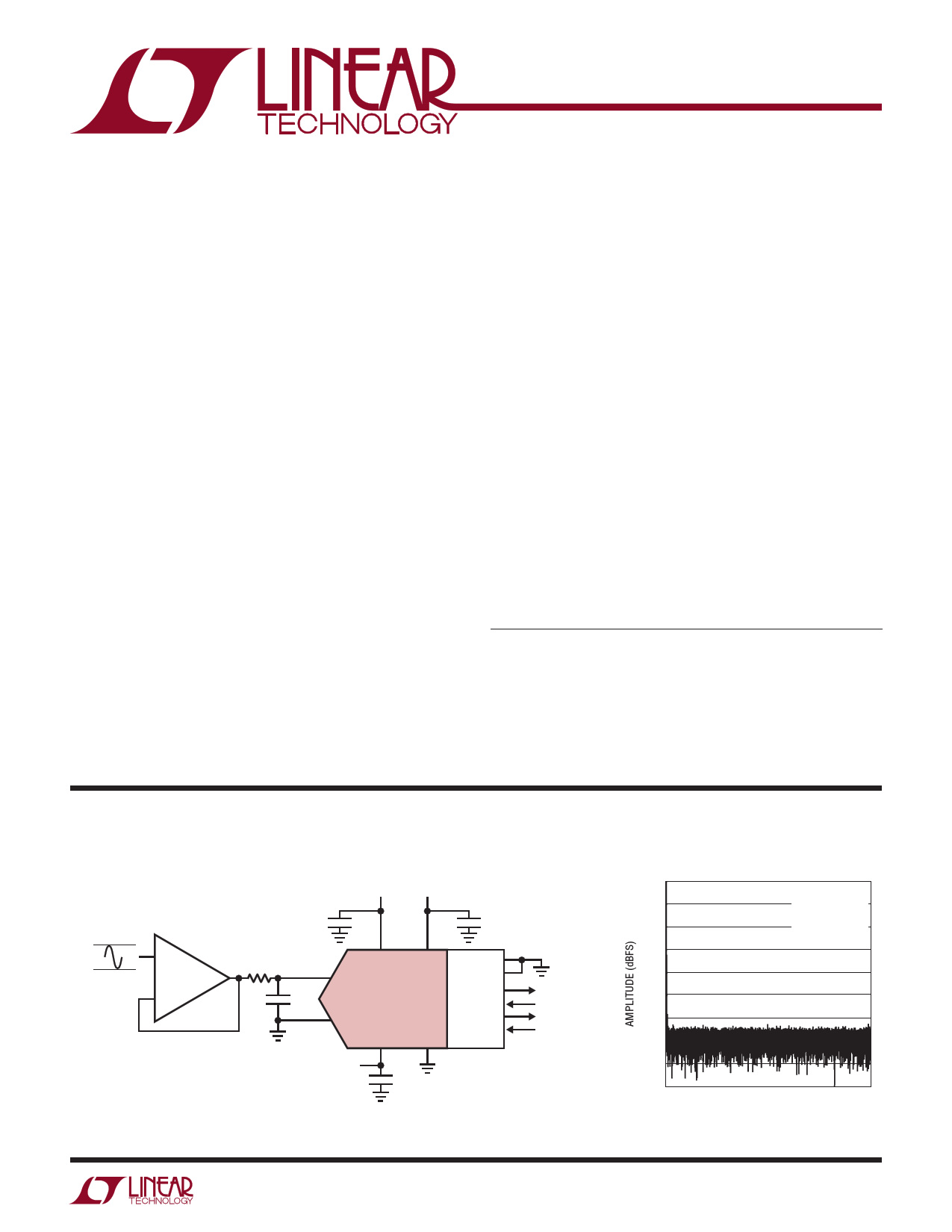
TYPICAL APPLICATION
2.5V 1.8V TO 5V
VREF
0V
+
LT®6202
–
10µF
0.1µF
10Ω
IN+
VDD
OVDD
CHAIN
RDL/SDI
10nF
LTC2368-16
SDO
SCK
IN– BUSY
REF GND CNV
2.5V TO 5.1V
236816 TA01a
47µF
(X5R, 0805 SIZE)
SAMPLE CLOCK
32k Point FFT fS = 1Msps, fIN = 2kHz
0
–20
–40
–60
–80
–100
–120
–140
–160
–180
0
SNR = 94.7dB
THD = –118dB
SINAD = 94.7dB
SFDR = 119dB
100 200 300 400 500
FREQUENCY (kHz)
236816 TA01b
236816f
1
1 page 
LTC2368-16
A DC TIMING CHARACTERISTICS The l denotes the specifications which apply over the full operating
temperature range, otherwise specifications are at TA = 25°C. (Note 4)
SYMBOL PARAMETER
CONDITIONS
MIN TYP
MAX UNITS
tSCKL
tSSDISCK
tHSDISCK
SCK Low Time
SDI Setup Time From SCK↑
SDI Hold Time From SCK↑
(Note 11)
(Note 11)
l4
l4
l1
ns
ns
ns
tSCKCH
tDSDO
SCK Period in Chain Mode
SDO Data Valid Delay from SCK↑
tSCKCH = tSSDISCK + tDSDO (Note 11)
CL = 20pF (Note 11)
l 13.5
l
ns
9.5 ns
tHSDO
SDO Data Remains Valid Delay from SCK↑
CL = 20pF (Note 10)
l1
ns
tDSDOBUSYL SDO Data Valid Delay from BUSY↓
tEN Bus Enable Time After RDL↓
CL = 20pF (Note 10)
(Note 11)
l
l
5 ns
16 ns
tDIS Bus Relinquish Time After RDL↑
(Note 11)
l 13 ns
Note 1: Stresses beyond those listed under Absolute Maximum Ratings
may cause permanent damage to the device. Exposure to any Absolute
Maximum Rating condition for extended periods may effect device
reliability and lifetime.
Note 2: All voltage values are with respect to ground.
Note 3: When these pin voltages are taken below ground or above REF or
OVDD, they will be clamped by internal diodes. This product can handle
input currents up to 100mA below ground or above REF or OVDD without
latch-up.
Note 4: VDD = 2.5V, OVDD = 2.5V, REF = 5V, fSMPL = 1MHz.
Note 5: Recommended operating conditions.
Note 6: Integral nonlinearity is defined as the deviation of a code from a
straight line passing through the actual endpoints of the transfer curve.
The deviation is measured from the center of the quantization band.
Note 7: Zero-scale error is the offset voltage measured from 0.5LSB
when the output code flickers between 0000 0000 0000 0000 and
0000 0000 0000 0001. Full-scale error is the deviation of the last code
transition from ideal and includes the effect of offset error.
Note 8: All specifications in dB are referred to a full-scale 5V input with a
5V reference voltage.
Note 9: fSMPL = 1MHz, IREF varies proportionately with sample rate.
Note 10: Guaranteed by design, not subject to test.
Note 11: Parameter tested and guaranteed at OVDD = 1.71V, OVDD = 2.5V
and OVDD = 5.25V.
Note 12: tSCK of 10ns maximum allows a shift clock frequency up to
100MHz for rising capture.
0.8*OVDD
tDELAY
0.8*OVDD
0.2*OVDD
0.2*OVDD
tDELAY
0.8*OVDD
0.2*OVDD
50%
tWIDTH
Figure 1. Voltage Levels for Timing Specifications
50%
236816 F01
236816f
5
5 Page 
LTC2368-16
APPLICATIONS INFORMATION
INPUT DRIVE CIRCUITS
A low impedance source can directly drive the high im-
pedance input of the LTC2368-16 without gain error. A
high impedance source should be buffered to minimize
settling time during acquisition and to optimize the dis-
tortion performance of the ADC. Minimizing settling time
is important even for DC inputs, because the ADC input
draws a current spike when entering acquisition.
For best performance, a buffer amplifier should be used
to drive the analog input of the LTC2368-16. The ampli-
fier provides low output impedance, which produces fast
settling of the analog signal during the acquisition phase.
It also provides isolation between the signal source and
the current spike the ADC input draws.
Input Filtering
The noise and distortion of the buffer amplifier and signal
source must be considered since they add to the ADC noise
and distortion. Noisy input signals should be filtered prior
to the buffer amplifier input with an appropriate filter to
minimize noise. The simple 1-pole RC lowpass filter (LPF1)
shown in Figure 4 is sufficient for many applications.
LPF1
VREF
50Ω
0V 66nF
+
LT6202
BW = 48kHz
–
LPF2
10Ω
10nF
IN+
LTC2368-16
IN–
BW = 1.6MHz
Figure 4. Input Signal Chain
236816 F04
Another filter network consisting of LPF2 should be used
between the buffer and ADC input to both minimize the
noise contribution of the buffer and to help minimize distur-
bances reflected into the buffer from sampling transients.
Long RC time constants at the analog inputs will slow
down the settling of the analog inputs. Therefore, LPF2
requires a wider bandwidth than LPF1. A buffer amplifier
with a low noise density must be selected to minimize
degradation of the SNR.
High quality capacitors and resistors should be used in the
RC filters since these components can add distortion. NPO
and silver mica type dielectric capacitors have excellent
linearity. Carbon surface mount resistors can generate
distortion from self heating and from damage that may
occur during soldering. Metal film surface mount resistors
are much less susceptible to both problems.
Pseudo-Differential Unipolar Inputs
For most applications, we recommend the low power
LT6202 ADC driver to drive the LTC2368-16. With a low
noise density of 1.9nV/√Hz and a low supply current of
3mA, the LT6202 is flexible and may be configured to
convert signals of various amplitudes to the 0V to 5V input
range of the LTC2368-16.
To achieve the full distortion performance of the
LTC2368‑16, a low distortion single-ended signal source
driven through the LT6202 configured as a unity-gain
buffer as shown in Figure 4 can be used to get the full
data sheet THD specification of –118dB.
The LT6202 can also be used to buffer and convert large
true bipolar signals which swing below ground to the 0V
to 5V input range of the LTC2368-16. Figure 5a shows the
LT6202 being used to convert a ±10V true bipolar signal
for use by the LTC2368-16. In this case, the LT6202 is
configured as an inverting amplifier stage, which acts to
attenuate and level shift the input signal to the 0V to 5V input
range of the LTC2368-16. In the inverting configuration, the
single-ended input signal source no longer directly drives
a high impedance input. The input impedance is instead
set by resistor RIN. RIN must be chosen carefully based on
the source impedance of the signal source. Higher values
of RIN tend to degrade both the noise and distortion of
the LT6202 and LTC2368-16 as a system. Table 1 shows
the resulting SNR and THD for several values of RIN, R1,
R2, R3 and R4 in this configuration. Figure 5b shows the
resulting FFT when using the LT6202 as shown in Figure 5a.
236816f
11
11 Page | ||
| Páginas | Total 24 Páginas | |
| PDF Descargar | [ Datasheet LTC2368-16.PDF ] | |
Hoja de datos destacado
| Número de pieza | Descripción | Fabricantes |
| LTC2368-16 | Pseudo-Differential Unipolar SAR ADC | Linear |
| Número de pieza | Descripción | Fabricantes |
| SLA6805M | High Voltage 3 phase Motor Driver IC. |
Sanken |
| SDC1742 | 12- and 14-Bit Hybrid Synchro / Resolver-to-Digital Converters. |
Analog Devices |
|
DataSheet.es es una pagina web que funciona como un repositorio de manuales o hoja de datos de muchos de los productos más populares, |
| DataSheet.es | 2020 | Privacy Policy | Contacto | Buscar |