|
|
|
PDF 7512 Data sheet ( Hoja de datos )
| Número de pieza | 7512 | |
| Descripción | SINGLE-CHIP 8-BIT CMOS MICROCOMPUTER | |
| Fabricantes | Renesas | |
| Logotipo | ||
Hay una vista previa y un enlace de descarga de 7512 (archivo pdf) en la parte inferior de esta página. Total 30 Páginas | ||
|
No Preview Available !
7512 Group
SINGLE-CHIP 8-BIT CMOS MICROCOMPUTER
REJ03B0122-0101
Rev.1.01
Feb 18, 2005
DESCRIPTION
The 7512 Group is the 8-bit microcomputer based on the 740 fam-
ily core technology.
The 7512 Group is designed for battery-pack and includes serial
interface functions, 8-bit timer, A/D converter, current integrator
and I2C-BUS interface.
FEATURES
qBasic machine-language instructions ...................................... 71
qMinimum instruction execution time .................................. 1.0 µs
(at 4 MHz oscillation frequency)
qMemory size
Flash memory .................................................. 36 K to 52 Kbytes
RAM ............................................................... 1.0 K to 1.5 Kbytes
qProgrammable input/output ports ............................................ 36
qInterrupts ................................................. 19 sources, 16 vectors
qTimers ............................................................................. 8-bit ✕ 4
qSerial interface
Serial I/O1 .......... 8-bit ✕ 1 (UART or Clock-synchronized)
Serial I/O2 .......................... 8-bit ✕ 1(Clock-synchronized)
qMulti-master I2C-BUS interface (option) ...................... 1 channel
qPWM ............................................................................... 8-bit ✕ 1
qA/D converter ............................................. 10-bit ✕ 10 channels
qCurrent integrator ......................................................... 1 channel
qOver current detector ................................................... 1 channel
qEasy thermal sensor .................................................... 1 channel
qWatchdog timer ............................................................ 16-bit ✕ 1
qClock generating circuit ..................................... Built-in 4 circuits
(high-speed RC oscillator and 32kHz RC oscillator, or connect to
external ceramic resonator or quartz-crystal oscillator)
qPower source voltage ............................................ 2.45 to 2.55 V
qPower dissipation
In high-speed mode ...................................................... 3.75 mW
(at 4 MHz oscillation frequency, at 2.5 V power source voltage)
In low-speed mode ........................................................ 1.05 mW
(at 32 kHz oscillation frequency, at 2.5 V power source voltage)
qOperating temperature range .................................... –20 to 85°C
APPLICATION
Battery-Pack, etc.
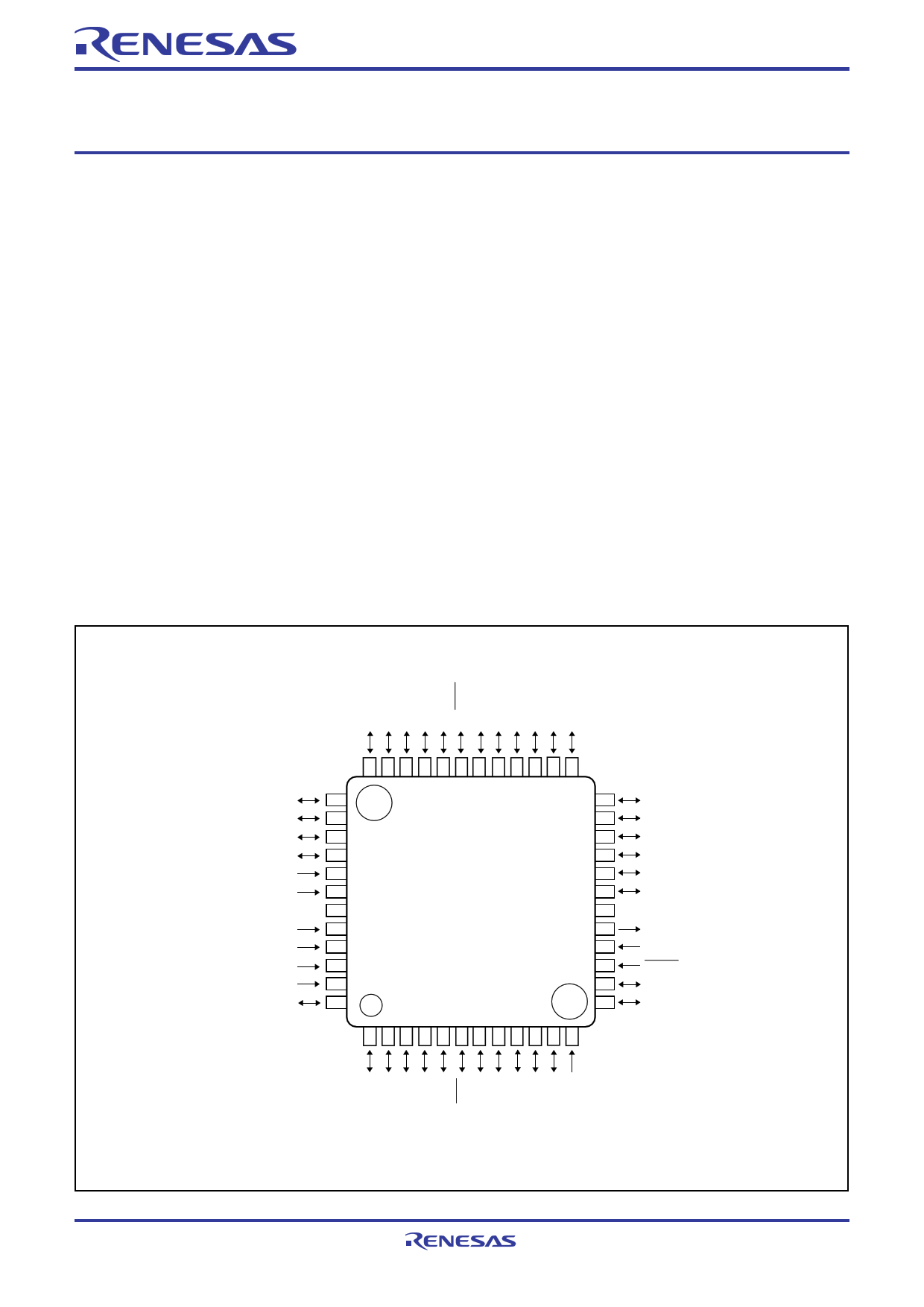
PIN CONFIGURATION (TOP VIEW)
P33/AN3
P32/AN2
P31/AN1
P30/AN0
ADVSS
ADVRED
VCC
AVCC
AVSS
ISENS0
ISENS1
DFETCNT/P45
37
38
39
40
41
42
43
44
45
46
47
48
M37512FCHP
24 P12/(LED2)
23 P13/(LED3)
22 P14/(LED4)
21 P15/(LED5)
20 P16/(LED6)
19 P17/(LED7)
18 VSS
17 XOUT
16 XIN
15 RESET
14 P20/XCOUT
13 P21/XCIN
Fig. 1 M37512FCHP pin configuration
Feb 18, 2005 page 1 of 85
REJ03B0122-0101
Package type : 48P6Q-A
1 page 
7512 Group
FUNCTIONAL DESCRIPTION
CENTRAL PROCESSING UNIT (CPU)
The 7512 Group uses the standard 740 Family instruction set. Re-
fer to the table of 740 Family addressing modes and machine
instructions or the 740 Family Software Manual for details on the
instruction set.
Machine-resident 740 Family instructions are as follows:
The FST and SLW instructions cannot be used.
The STP, WIT, MUL, and DIV instructions can be used.
[Accumulator (A)]
The accumulator is an 8-bit register. Data operations such as data
transfer, etc. are executed mainly through the accumulator.
[Index Register X (X)]
The index register X is an 8-bit register. In the index addressing
modes, the value of the OPERAND is added to the contents of
register X and specifies the real address.
[Index Register Y (Y)]
The index register Y is an 8-bit register. In partial instruction, the
value of the OPERAND is added to the contents of register Y and
specifies the real address.
[Stack Pointer (S)]
The stack pointer is an 8-bit register used during subroutine calls
and interrupts. This register indicates start address of stored area
(stack) for storing registers during subroutine calls and interrupts.
The low-order 8 bits of the stack address are determined by the
contents of the stack pointer. The high-order 8 bits of the stack ad-
dress are determined by the stack page selection bit. If the stack
page selection bit is “0” , the high-order 8 bits becomes “0016”. If
the stack page selection bit is “1”, the high-order 8 bits becomes
“0116”.
The operations of pushing register contents onto the stack and
popping them from the stack are shown in Figure 5.
Store registers other than those described in Figure 4 with pro-
gram when the user needs them during interrupts or subroutine
calls (see Table 3).
[Program Counter (PC)]
The program counter is a 16-bit counter consisting of two 8-bit
registers PCH and PCL. It is used to indicate the address of the
next instruction to be executed.
b15
PCH
b7 b0
A Accumulator
b7 b0
X Index register X
b7 b0
Y Index register Y
b7 b0
S Stack pointer
b7 b0
PCL Program counter
b7 b0
N V T B D I Z C Processor status register (PS)
Carry flag
Zero flag
Interrupt disable flag
Decimal mode flag
Break flag
Index X mode flag
Overflow flag
Negative flag
Fig.4 740 Family CPU register structure
Feb 18, 2005 page 5 of 85
REJ03B0122-0101
5 Page 
7512 Group
I/O PORTS
The I/O ports have direction registers which determine the input/
output direction of each individual pin. Each bit in a direction reg-
ister corresponds to one pin, and each pin can be set to be input
port or output port.
When “0” is written to the bit corresponding to a pin, that pin be-
comes an input pin. When “1” is written to that bit, that pin
becomes an output pin.
If data is read from a pin which is set to output, the value of the
port output latch is read, not the value of the pin itself. Pins set to
input are floating. If a pin set to input is written to, only the port
output latch is written to and the pin remains floating.
Table 5 I/O port function
Pin Name
P00/SIN2
Port P0
P01/SOUT2
P02/SCLK2
__________
P03/SRDY2
P04/AN8
P05/AN9
P06/CFETCNT/AN10
P07/AN11/PWM1
P10–P17
Port P1
P20/XCOUT
P21/XCIN
P22/SDA1
P23/SCL1
P24/SDA2/RxD
P25/SCL2/TxD
Port P2
Input/Output
I/O Structure
Non-Port Function
Related SFRs
Input/output, CMOS compatible input level Serial I/O2 function I/O Serial I/O2 control register
individual bits CMOS 3-state output
A/D conversion input AD control register
MISRG2
A/D conversion input AD control register, MISRG2
Over current detector Charge over current detect
output
control register
A/D conversion input AD control register, MISRG2
PWM output
PWM control register
CMOS compatible input level
N-channel open-drain output
CMOS compatible input level Sub-clock generating CPU mode register
CMOS 3-state output
circuit
CMOS compatible input level I2C-BUS interface
MISRG2
I2C control register
CMOS/SMBUS input level function I/O
(when selecting I2C-BUS I2C-BUS interface
I2C control register
interface function)
function I/O
Serial I/O1 control register
N-channel open-drain output Serial I/O1 function I/O
Ref.No.
(1)
(2)
(3)
(4)
(5)
(6)
(7)
(8)
(9)
(10)
(11)
(12)
(13)
(14)
(15)
P26/SCLK
P27/CNTR0/
__________
SRDY1
P30/AN0–
P35/AN5
P40/CNTR1
P41/INT0
P42/INT1
P43/INT2/SCMP2
Port P3
Port P4
P44/INT3/PWM0
P45/DFETCNT
CMOS compatible input level Serial I/O1 function I/O Serial I/O1 control register
CMOS 3-state output
Serial I/O1 function I/O Serial I/O1 control register
Timer X function I/O Timer XY mode register
A/D conversion input AD control register
MISRG2
Timer Y function I/O Timer XY mode register
External interrupt input Interrupt edge selection
register 1
CMOS compatible input level External interrupt input Interrupt edge selection
N-channel open-drain output SCMP2 output
register 2
Serial I/O2 control register
External interrupt input Interrupt edge selection
PWM output
register 2
PWM control register
CMOS compatible input level Over current detector Short current detect control
CMOS 3-state output
output
register
Over current detect control
register
Wake up current detect
control register
(16)
(17)
(6)
(18)
(19)
(20)
(21)
(22)
Feb 18, 2005 page 11 of 85
REJ03B0122-0101
11 Page | ||
| Páginas | Total 30 Páginas | |
| PDF Descargar | [ Datasheet 7512.PDF ] | |
Hoja de datos destacado
| Número de pieza | Descripción | Fabricantes |
| 7512 | SINGLE-CHIP 8-BIT CMOS MICROCOMPUTER | Renesas |
| 75185 | MULTIPLE RS-232 DRIVERS AND RECEIVERS | Unisonic Technologies |
| 75190 | PRESETTABLE BCD/DECADE UP/DOWN COUNTERS | Motorola Semiconductors |
| 75191 | PRESETTABLE BCD/DECADE UP/DOWN COUNTERS | Motorola Semiconductors |
| Número de pieza | Descripción | Fabricantes |
| SLA6805M | High Voltage 3 phase Motor Driver IC. |
Sanken |
| SDC1742 | 12- and 14-Bit Hybrid Synchro / Resolver-to-Digital Converters. |
Analog Devices |
|
DataSheet.es es una pagina web que funciona como un repositorio de manuales o hoja de datos de muchos de los productos más populares, |
| DataSheet.es | 2020 | Privacy Policy | Contacto | Buscar |