|
|
PDF GC8051 Data sheet ( Hoja de datos )
| Número de pieza | GC8051 | |
| Descripción | 1 Cell Li-Ion Battery Charger | |
| Fabricantes | GammaComm | |
| Logotipo |  |
|
Hay una vista previa y un enlace de descarga de GC8051 (archivo pdf) en la parte inferior de esta página. Total 12 Páginas | ||
|
No Preview Available !
1 Cell Li-Ion Battery Charger
GC1261 Data Sheet Information
单颗锂电池充电管理芯片
[GC8051 IC Specification]
Smart Battery
Charging
with
GC8051
REV 1.0 11/03/2005
www.gammacommtech.com
Characteristics subject to change without notice. 1 of 12
1 page 
GC3001A Data Sheet Information
8. Absolute Maximum Ratings
Input voltage between VDD and VSS -------------------------------------------------- VSS -0.3 V to VSS +12 V
Input pin voltage for VM -------------------------------------------------------------- VDD -30 V to VDD +0.3 V
Output pin voltage for CO ------------------------------------------------------------- VVM -0.3 V to VDD +0.3 V
Output pin voltage for DO --------------------------------------------------------------- VSS -0.3 V to VDD +0.3 V
Power dissipation SOT-23-6 ----------------------------------------------------------------------------
250mW
Operating temperature range --------------------------------------------------------------------- -40°C to +85°C
Storage temperature range --------------------------------------------------------------------- -55°C to +125°C
ESD Susceptibility
HBM (Human Body Mode) -------------------------------------------------------------------------------
>1KV
MM (Machine Mode) ---------------------------------------------------------------------------------------
>200V
9. Ordering Information
Order Number
Package Type
GC8051-41MIR1
MSOP-8
GC8051-41MIR0
MSOP-8
GC8051-42MIR1
MSOP-8
GC8051-42MIR0
MSOP-8
Marking
xxxx
8051
xxxx
8051
xxxx
8051C
xxxx
8051C
Operating Temperature range
-20 °C to 70°C
-20 °C to 70°C
-20 °C to 70°C
-20 °C to 70°C
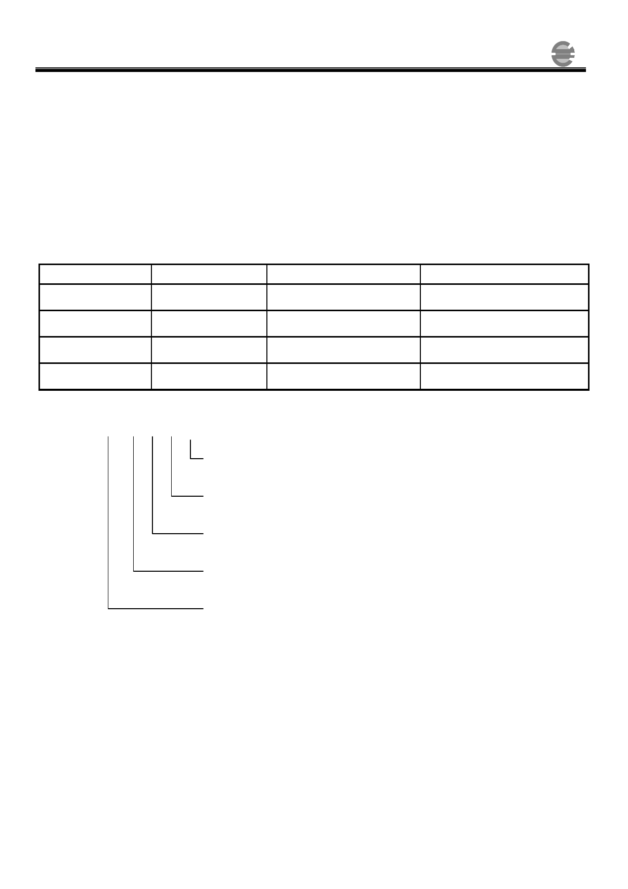
GC8051-□ □ □ □ □ □
Lead Free Code
1: Lead Free 0: Lead
Packing
R: Tape& Reel
Operating temperature range
I: Industry Standard
Package Type
M: MSOP
Output Voltage
41: 4.1V
42: 4.2V
REV 1.0 11/03/2005
www.gammacommtech.com
Characteristics subject to change without notice. 5 of 12
5 Page 
GC3001A Data Sheet Information
27. P-Channel MOSFET
Selection steps for a P-channel MOSFET: We will use the following conditions: VI=5V (with 10% supply
tolerance); I(REG)=1A, 4.2-V single-cell Li-Ion. VI is the input voltage to the charger and I(REG) is the desired
charge current. (See Figure2)
1. Determine the maximum power dissipation, PD , in
the transistor.
The worst case power dissipation happens when the cell voltage, V(constant), is at its lowest (typically 3.1V at
the beginning of current regulation phase) and VI is at its maximum. Where VD is the forward voltage drop
across the reverse-blocking diode (if one is used), and VCS is the voltage drop across the current sense
resistor.
PD=(VI(MAX)-VD-VCS-VBAT)×IREG --------- (7)
PD=(5.5-0.4-0.2-3.1)×1A
PD=1.8W
2. Determine the package size needed in order to keep
the junction temperature below the manufacturer’s recommended value, TJMAX. Calculate the total theta,
θ(°C/W), needed.
θ JA
=
(Tmax(J) - TA(max) )
PD
--------------(8)
θ JA
=
(150 - 40)
1.8
θJA = 61°C/W
It is recommended to choose a package with a lower θJA than the number calculated above.
3. Select a drain-source voltage, V(DS), rating greater
than the maximum input voltage. A 12V device will be adequate in this example.
4. Select a device that has at least 50% higher drain
current (ID) rating than the desired charge current I(REG).
5. Verify that the available drive is large enough to
supply the desired charge current.
V(GS)=(VD+V(CS)+VOL(CC))-VI(min)
V(GS)=(0.4+0.2+1) - 4.5
V(GS)=-2.9
-------------- (9)
Where V(GS) is the gate-to-source voltage, VD is the forward voltage drop across the reverse-blocking diode (if
one is used), and VCS is the voltage drop across the current sense resistor, and VOL(CC) is the CC pin output
low voltage specification for the GC8051.
Select a MOSFET with gate threshold voltage, V(GSth), rating less than the calculated V(GS).
28. Reverse Blocking Protection
The optional reverse-blocking protection diode, depicted in Figure1&2 provides protection from a faulted or
shorted input, or from a reversed-polarity input source. Without the protection diode, a faulted of shorted
input would discharge the battery pack through the body diode of the external pass transistor.
If a reverse-protection diode is incorporated in the design, it should be chosen to handle the fast charge
current continuously at the maximum ambient temperature. In addition, the reverse-leakage current of the
diode should be kept as small as possible.
REV 1.0 11/03/2005
www.gammacommtech.com
Characteristics subject to change without notice. 11 of 12
11 Page | ||
| Páginas | Total 12 Páginas | |
| PDF Descargar | [ Datasheet GC8051.PDF ] | |
Hoja de datos destacado
| Número de pieza | Descripción | Fabricantes |
| GC80503 | Low Power Embedded Processor | Intel |
| GC8051 | 1 Cell Li-Ion Battery Charger | GammaComm |
| Número de pieza | Descripción | Fabricantes |
| SLA6805M | High Voltage 3 phase Motor Driver IC. |
Sanken |
| SDC1742 | 12- and 14-Bit Hybrid Synchro / Resolver-to-Digital Converters. |
Analog Devices |
|
DataSheet.es es una pagina web que funciona como un repositorio de manuales o hoja de datos de muchos de los productos más populares, |
| DataSheet.es | 2020 | Privacy Policy | Contacto | Buscar |
