|
|
|
PDF STP7LN80K5 Data sheet ( Hoja de datos )
| Número de pieza | STP7LN80K5 | |
| Descripción | N-channel Power MOSFET | |
| Fabricantes | STMicroelectronics | |
| Logotipo | ||
Hay una vista previa y un enlace de descarga de STP7LN80K5 (archivo pdf) en la parte inferior de esta página. Total 13 Páginas | ||
|
No Preview Available !
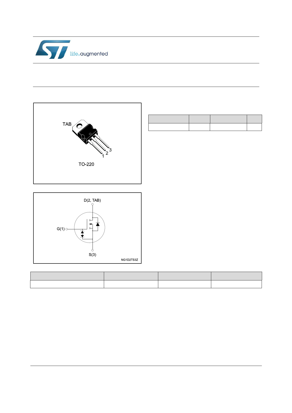
STP7LN80K5
N-channel 800 V, 0.95 Ω typ., 5 A MDmesh™ K5
Power MOSFET in a TO-220 package
Datasheet - production data
Figure 1: Internal schematic diagram
Features
Order code
STP7LN80K5
VDS
800 V
RDS(on) max.
1.15 Ω
ID
5A
Industry’s lowest RDS(on) x area
Industry’s best figure of merit (FoM)
Ultra-low gate charge
100% avalanche tested
Zener-protected
Applications
Switching applications
Description
This very high voltage N-channel Power
MOSFET is designed using MDmesh™ K5
technology based on an innovative proprietary
vertical structure. The result is a dramatic
reduction in on-resistance and ultra-low gate
charge for applications requiring superior power
density and high efficiency.
Order code
STP7LN80K5
Table 1: Device summary
Marking
Package
7LN80K5
TO-220
Packing
Tube
January 2016
DocID028826 Rev 1
This is information on a product in full production.
1/13
www.st.com
1 page 
STP7LN80K5
Symbol
Parameter
Table 8: Source drain diode
Test conditions
Electrical characteristics
Min. Typ. Max. Unit
ISD
ISDM(1)
VSD (2)
trr
Qrr
IRRM
Source-drain current
Source-drain current
(pulsed)
Forward on voltage
Reverse recovery time
Reverse recovery
charge
Reverse recovery
current
ISD= 5 A, VGS = 0 V
ISD = 5 A, di/dt = 100 A/µs,
VDD = 60 V (see Figure 16: "Test
circuit for inductive load
switching and diode recovery
times")
- 5A
- 20 A
- 1.6 V
- 276
ns
- 2.13
µC
- 15.4
A
trr Reverse recovery time
Qrr
Reverse recovery
charge
IRRM
Reverse recovery
current
ISD = 5 A, di/dt = 100 A/µs,
VDD = 60 V, Tj = 150 °C
(see Figure 16: "Test circuit for
inductive load switching and
diode recovery times")
- 402
- 2.79
- 13.9
ns
µC
A
Notes:
(1)Pulse width is limited by safe operating area
(2)Pulsed: pulse duration = 300 µs, duty cycle 1.5%
Symbol
V(BR)GSO
Table 9: Gate-source Zener diode
Parameter
Test conditions
Gate-source breakdown voltage IGS = ±1 mA, ID = 0 A
Min. Typ. Max. Unit
30 -
V
The built-in back-to-back Zener diodes are specifically designed to enhance the ESD
performance of the device. The Zener voltage facilitates efficient and cost-effective device
integrity protection,thus eliminating the need for additional external componentry.
DocID028826 Rev 1
5/13
5 Page 
STP7LN80K5
Dim.
A
b
b1
c
D
D1
E
e
e1
F
H1
J1
L
L1
L20
L30
øP
Q
Table 10: TO-220 type A mechanical data
mm
Min.
Typ.
4.40
0.61
1.14
0.48
15.25
10
2.40
4.95
1.23
6.20
2.40
13
3.50
3.75
2.65
1.27
16.40
28.90
Package information
Max.
4.60
0.88
1.70
0.70
15.75
10.40
2.70
5.15
1.32
6.60
2.72
14
3.93
3.85
2.95
DocID028826 Rev 1
11/13
11 Page | ||
| Páginas | Total 13 Páginas | |
| PDF Descargar | [ Datasheet STP7LN80K5.PDF ] | |
Hoja de datos destacado
| Número de pieza | Descripción | Fabricantes |
| STP7LN80K5 | N-channel Power MOSFET | STMicroelectronics |
| Número de pieza | Descripción | Fabricantes |
| SLA6805M | High Voltage 3 phase Motor Driver IC. |
Sanken |
| SDC1742 | 12- and 14-Bit Hybrid Synchro / Resolver-to-Digital Converters. |
Analog Devices |
|
DataSheet.es es una pagina web que funciona como un repositorio de manuales o hoja de datos de muchos de los productos más populares, |
| DataSheet.es | 2020 | Privacy Policy | Contacto | Buscar |