|
|
|
PDF STH6N95K5-2 Data sheet ( Hoja de datos )
| Número de pieza | STH6N95K5-2 | |
| Descripción | N-channel Power MOSFET | |
| Fabricantes | STMicroelectronics | |
| Logotipo | ||
Hay una vista previa y un enlace de descarga de STH6N95K5-2 (archivo pdf) en la parte inferior de esta página. Total 17 Páginas | ||
|
No Preview Available !
STH6N95K5-2
N-channel 950 V, 1 Ω typ., 6 A MDmesh™ K5
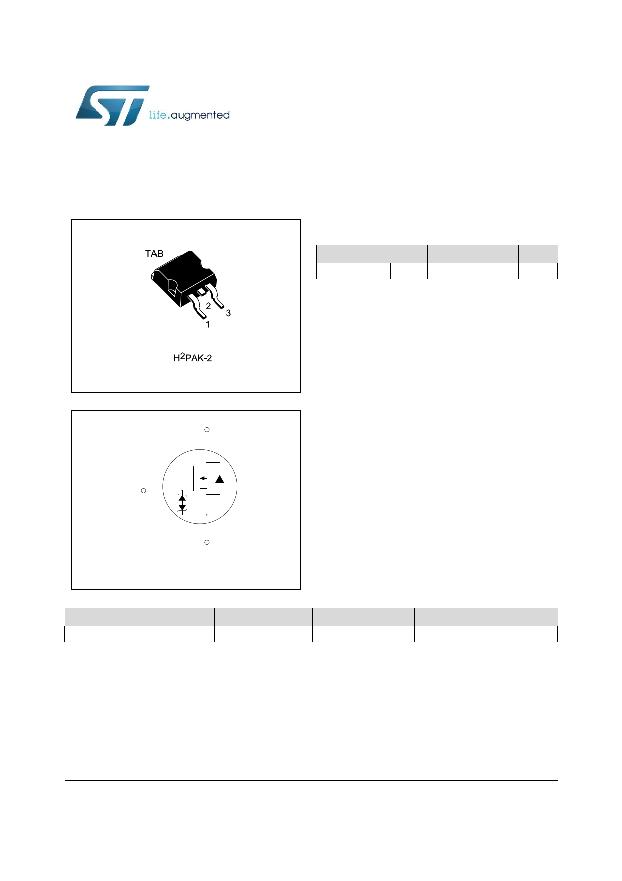
Power MOSFET in a H²PAK-2 package
Datasheet - production data
Figure 1: Internal schematic diagram
D(TAB)
G(1)
Features
Order code
VDS RDS(on) max. ID
PTOT
STH6N95K5-2 950 V
1.25 Ω
6 A 110 W
Industry’s lowest RDS(on) x area
Industry’s best figure of merit (FoM)
Ultra low gate charge
100% avalanche tested
Zener-protected
Applications
Switching applications
Description
This very high voltage N-channel Power
MOSFET is designed using MDmesh™ K5
technology based on an innovative proprietary
vertical structure. The result is a dramatic
reduction in on-resistance and ultra-low gate
charge for applications requiring superior power
density and high efficiency.
S(2, 3)
Order code
STH6N95K5-2
AM15557a.v3
Table 1: Device summary
Marking
Package
6N95K5
H²PAK-2
Packaging
Tape and reel
March 2015
DocID027383 Rev 3
This is information on a product in full production.
1/17
www.st.com
1 page 
STH6N95K5-2
Electrical characteristics
Symbol
ISD
ISDM(1)
VSD(2)
trr
Qrr
IRRM
trr
Qrr
IRRM
Table 7: Source drain diode
Parameter
Test conditions
Source-drain current
Source-drain current (pulsed)
Forward on voltage
Reverse recovery time
Reverse recovery charge
Reverse recovery current
ISD = 6 A, VGS = 0
ISD = 6 A,
di/dt = 100 A/µs
VDD = 60 V
Reverse recovery time
Reverse recovery charge
Reverse recovery current
ISD = 6 A,
di/dt = 100 A/µs
VDD = 60 V, Tj = 150 °C
Notes:
(1)Pulse width limited by safe operating area
(2)Pulsed: pulse duration = 300 µs, duty cycle 1.5%
Min.
-
-
-
-
-
-
-
-
-
Typ.
372
4
22
522
5
20
Max.
6
24
1.6
Unit
A
A
V
ns
µC
A
ns
µC
A
Symbol
V(BR)GSO
Parameter
Table 8: Gate-source Zener diode
Test conditions
Gate-source breakdown voltage
IGS = ± 1mA, ID=0
Min.
30
Typ.
-
Max.
-
Unit
V
The built-in back-to-back Zener diodes have specifically been designed to enhance the
device's ESD capability. In this respect the Zener voltage is appropriate to achieve an
efficient and cost-effective intervention to protect the device's integrity. These integrated
Zener diodes thus avoid the usage of external components.
DocID027383 Rev 3
5/17
5 Page 
STH6N95K5-2
4.1 Package mechanical data
Figure 21: H²PAK-2 outline
Package mechanical data
DocID027383 Rev 3
8159712_D
11/17
11 Page | ||
| Páginas | Total 17 Páginas | |
| PDF Descargar | [ Datasheet STH6N95K5-2.PDF ] | |
Hoja de datos destacado
| Número de pieza | Descripción | Fabricantes |
| STH6N95K5-2 | N-channel Power MOSFET | STMicroelectronics |
| Número de pieza | Descripción | Fabricantes |
| SLA6805M | High Voltage 3 phase Motor Driver IC. |
Sanken |
| SDC1742 | 12- and 14-Bit Hybrid Synchro / Resolver-to-Digital Converters. |
Analog Devices |
|
DataSheet.es es una pagina web que funciona como un repositorio de manuales o hoja de datos de muchos de los productos más populares, |
| DataSheet.es | 2020 | Privacy Policy | Contacto | Buscar |