|
|
|
PDF STB37N60DM2AG Data sheet ( Hoja de datos )
| Número de pieza | STB37N60DM2AG | |
| Descripción | N-channel Power MOSFET | |
| Fabricantes | STMicroelectronics | |
| Logotipo | ||
Hay una vista previa y un enlace de descarga de STB37N60DM2AG (archivo pdf) en la parte inferior de esta página. Total 15 Páginas | ||
|
No Preview Available !
STB37N60DM2AG
Automotive-grade N-channel 600 V, 0.094 Ω typ., 28 A
MDmesh™ DM2 Power MOSFET in a D²PAK package
Datasheet - production data
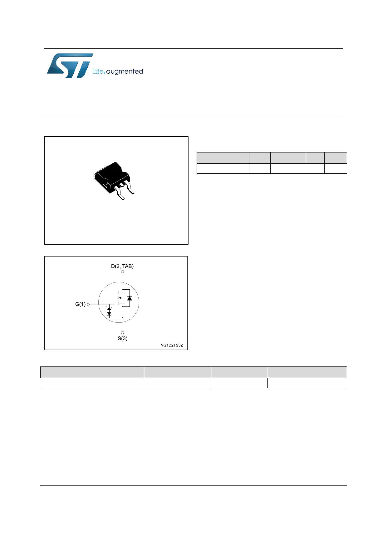
TAB
Features
Order code
STB37N60DM2AG
VDS
600 V
RDS(on) max.
0.110 Ω
ID
28 A
PTOT
210 W
3
1
D2PAK
Figure 1: Internal schematic diagram
Designed for automotive applications and
AEC-Q101 qualified
Fast-recovery body diode
Extremely low gate charge and input
capacitance
Low on-resistance
100% avalanche tested
Extremely high dv/dt ruggedness
Zener-protected
Applications
Switching applications
Order code
STB37N60DM2AG
Description
This high voltage N-channel Power MOSFET is
part of the MDmesh™ DM2 fast recovery diode
series. It offers very low recovery charge (Qrr)
and time (trr) combined with low RDS(on), rendering
it suitable for the most demanding high efficiency
converters and ideal for bridge topologies and
ZVS phase-shift converters.
Table 1: Device summary
Marking
Package
Packing
37N60DM2
D²PAK
Tape and reel
August 2015
DocID028271 Rev 1
This is information on a product in full production.
1/15
www.st.com
1 page 
STB37N60DM2AG
Symbol
ISD
ISDM(1)
VSD(2)
trr
Qrr
IRRM
trr
Qrr
IRRM
Parameter
Table 8: Source-drain diode
Test conditions
Electrical characteristics
Min. Typ. Max. Unit
Source-drain current
- 28 A
Source-drain current
(pulsed)
- 112 A
Forward on voltage
Reverse recovery
time
Reverse recovery
charge
Reverse recovery
current
VGS = 0 V, ISD = 28 A
ISD = 28 A, di/dt = 100 A/µs,
VDD = 60 V (see Figure 16: "Test
circuit for inductive load
switching and diode recovery
times")
- 1.6 V
- 120
ns
- 572
nC
- 10.2
A
Reverse recovery
time
Reverse recovery
charge
Reverse recovery
current
ISD = 28 A, di/dt = 100 A/µs,
VDD = 60 V, Tj = 150 °C (see
Figure 16: "Test circuit for
inductive load switching and
diode recovery times")
- 215
- 1.89
- 17.7
ns
µC
A
Notes:
(1) Pulse width is limited by safe operating area.
(2) Pulse test: pulse duration = 300 µs, duty cycle 1.5%.
Symbol
V(BR)GSO
Table 9: Gate-source Zener diode
Parameter
Test conditions
Gate-source breakdown voltage IGS = ±250 µA, ID = 0 A
Min. Typ. Max. Unit
±30 -
-V
The built-in back-to-back Zener diodes are specifically designed to enhance the ESD
performance of the device. The Zener voltage facilitates efficient and cost-effective device
integrity protection, thus eliminating the need for additional external componentry.
DocID028271 Rev 1
5/15
5 Page 
STB37N60DM2AG
Package information
Figure 21: D²PAK (TO-263) recommended footprint (dimensions are in mm)
DocID028271 Rev 1
11/15
11 Page | ||
| Páginas | Total 15 Páginas | |
| PDF Descargar | [ Datasheet STB37N60DM2AG.PDF ] | |
Hoja de datos destacado
| Número de pieza | Descripción | Fabricantes |
| STB37N60DM2AG | N-channel Power MOSFET | STMicroelectronics |
| Número de pieza | Descripción | Fabricantes |
| SLA6805M | High Voltage 3 phase Motor Driver IC. |
Sanken |
| SDC1742 | 12- and 14-Bit Hybrid Synchro / Resolver-to-Digital Converters. |
Analog Devices |
|
DataSheet.es es una pagina web que funciona como un repositorio de manuales o hoja de datos de muchos de los productos más populares, |
| DataSheet.es | 2020 | Privacy Policy | Contacto | Buscar |