|
|
|
PDF NCL30088 Data sheet ( Hoja de datos )
| Número de pieza | NCL30088 | |
| Descripción | Power Factor Corrected Quasi-Resonant Primary Side Current-Mode Controller | |
| Fabricantes | ON Semiconductor | |
| Logotipo | ||
Hay una vista previa y un enlace de descarga de NCL30088 (archivo pdf) en la parte inferior de esta página. Total 26 Páginas | ||
|
No Preview Available !
NCL30088
Power Factor Corrected
Quasi-Resonant Primary
Side Current-Mode
Controller for LED Lighting
with Thermal Foldback
The NCL30088 is a power factor corrected flyback controller
targeting isolated and non−isolated constant current LED drivers. The
controller operates in a quasi−resonant mode to provide optimal
efficiency. Thanks to a novel control method, the device is able to
tightly regulate a constant LED current from the primary side. This
removes the need for secondary side feedback circuitry, biasing and an
optocoupler.
The device is highly integrated with a minimum number of external
components. A robust suite of safety protection is built in to simplify
the design. This device is specifically intended for very compact,
space efficient designs.
Features
• Quasi−resonant Peak Current−mode Control Operation
• Constant Current Control with Primary Side Feedback
• Tight LED Constant Current Regulation of ±2% Typical
• Power Factor Correction
• Line Feedforward for Enhanced Regulation Accuracy
• Low Start−up Current (13 mA typ.)
• Wide Vcc Range
• 300 mA / 500 mA Totem Pole Driver with 12 V Gate Clamp
• Robust Protection Features
♦ OVP on VCC
♦ Programmable Over Voltage / LED Open Circuit Protection
♦ Cycle−by−cycle Peak Current Limit
♦ Winding Short Circuit Protection
♦ Secondary Diode Short Protection
♦ Output Short Circuit Protection
♦ Shorted Current Sense Protection
♦ User Programmable NTC Based Thermal Foldback
♦ Thermal Shutdown
♦ Vcc Undervoltage Lockout
♦ Brown−out Protection
• Pb−Free, Halide−Free Product
• Four Versions: NCL30088A, B, C and D (See Table 1)
Typical Applications
• Integral LED Bulbs and Tubes
• LED Light Engines
• LED Drivers/Power Supplies
• Electronic Control Gear for LED Lighting
www.onsemi.com
8
1
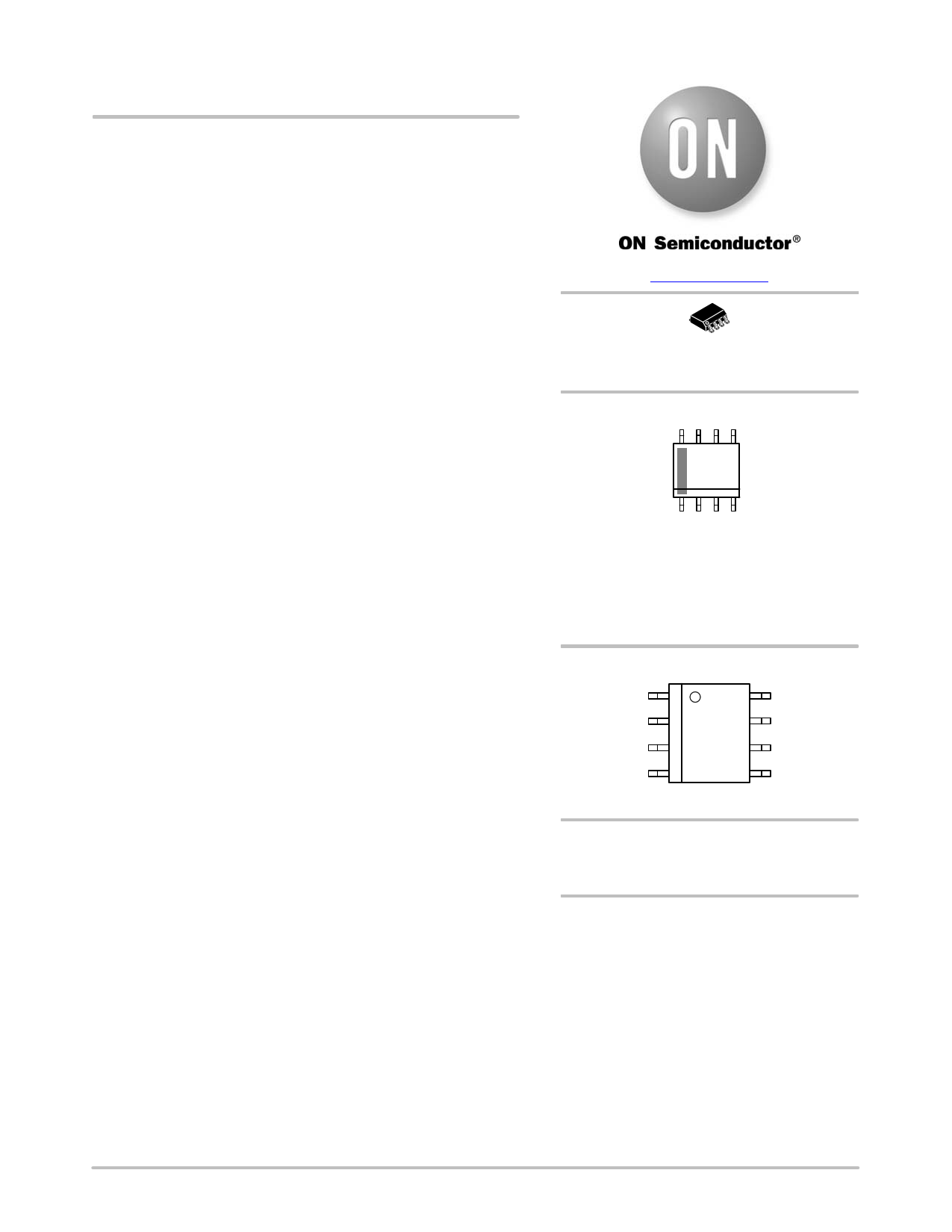
SOIC−8 NB
CASE 751
MARKING DIAGRAM
8
L30088x
ALYW
G
1
L30088x = Specific Device Code
x = A, B, C, D
A = Assembly Location
L = Wafer Lot
Y = Year
W = Work Week
G = Pb-Free Package
PIN CONNECTIONS
1
ZCD
VCC
VS DRV
COMP
GND
SD CS
(Top View)
ORDERING INFORMATION
See detailed ordering and shipping information in the package
dimensions section on page 25 of this data sheet.
© Semiconductor Components Industries, LLC, 2015
April, 2015 − Rev. 4
1
Publication Order Number:
NCL30088/D
1 page 
NCL30088
Table 3. MAXIMUM RATINGS TABLE
Symbol
Rating
Value
Unit
VCC(MAX)
ICC(MAX)
Maximum Power Supply voltage, VCC pin, continuous voltage
Maximum current for VCC pin
−0.3 to 30
Internally limited
V
mA
VDRV(MAX)
IDRV(MAX)
VMAX
IMAX
RθJ−A
TJ(MAX)
Maximum driver pin voltage, DRV pin, continuous voltage
Maximum current for DRV pin
Maximum voltage on low power pins (except DRV and VCC pins)
Current range for low power pins (except DRV and VCC pins)
Thermal Resistance Junction−to−Air
Maximum Junction Temperature
Operating Temperature Range
−0.3, VDRV (Note 1)
−300, +500
−0.3, 5.5 (Notes 2 and 5)
−2, +5
180
150
−40 to +125
V
mA
V
mA
°C/W
°C
°C
Storage Temperature Range
−60 to +150
°C
ESD Capability, HBM model (Note 3)
3.5 kV
ESD Capability, MM model (Note 3)
250 V
ESD Capability, CDM model (Note 3)
2 kV
Stresses exceeding those listed in the Maximum Ratings table may damage the device. If any of these limits are exceeded, device functionality
should not be assumed, damage may occur and reliability may be affected.
1. VDRV is the DRV clamp voltage VDRV(high) when VCC is higher than VDRV(high). VDRV is VCC otherwise.
2. This level is low enough to guarantee not to exceed the internal ESD diode and 5.5−V Zener diode. More positive and negative voltages can
be applied if the pin current stays within the −2−mA / 5−mA range.
3. This device contains ESD protection and exceeds the following tests: Human Body Model 3500 V per JEDEC Standard JESD22−A114E,
Machine Model Method 250 V per JEDEC Standard JESD22−A115B, Charged Device Model 2000 V per JEDEC Standard JESD22−C101E.
4. This device contains latch−up protection and has been tested per JEDEC Standard JESD78D, Class I and exceeds ±100 mA
5. Recommended maximum VS voltage for optimal operation is 4 V. −0.3 V to +4.0 V is hence, the VS pin recommended range.
Table 4. ELECTRICAL CHARACTERISTICS (Unless otherwise noted: For typical values TJ = 25°C, VCC = 12 V, VZCD = 0 V,
VCS = 0 V, VSD = 1.5 V) For min/max values TJ = −40°C to +125°C, VCC = 12 V)
Description
Test Condition
Symbol
Min Typ Max Unit
STARTUP AND SUPPLY CIRCUITS
Supply Voltage
Startup Threshold
Minimum Operating Voltage
Hysteresis VCC(on) – VCC(off)
Internal logic reset
VCC Over Voltage Protection Threshold
VCC(off) noise filter
VCC(reset) noise filter
Startup current
Startup current in fault mode
Supply Current
Device Disabled/Fault
Device Enabled/No output load on pin 7
Device Switching (FSW = 65 kHz)
CURRENT SENSE
VCC rising
VCC rising
VCC falling
VCC(on)
VCC(off)
VCC(HYS)
VCC(reset)
VCC(OVP)
tVCC(off)
tVCC(reset)
ICC(start)
ICC(sFault)
16.0
8.2
8
4
25.5
−
−
−
18.0
8.8
−
5
26.8
5
20
13
58
20.0
9.4
−
6
28.5
−
−
30
75
VCC > VCC(off)
Fsw = 65 kHz
CDRV = 470 pF, Fsw = 65 kHz
ICC1
ICC2
ICC3
0.8 1.0 1.2
– 2.6 4.0
− 3.0 4.5
V
V
ms
mA
mA
mA
Maximum Internal current limit
VILIM
0.95 1.00 1.05
V
Leading Edge Blanking Duration for VILIM
tLEB
240 300 360
ns
6. Guaranteed by Design
7. A NTC is generally placed between the SD and GND pins. Parameters RTF(start), RTF(stop), ROTP(off) and ROTP(on) give the resistance the
NTC must exhibit to respectively, enter thermal foldback, stop thermal foldback, trigger the OTP limit and allow the circuit recovery after
an OTP situation.
8. At startup, when VCC reaches VCC(on), the controller blanks OTP for more than 250 ms to avoid detecting an OTP fault by allowing the
SD pin voltage to reach its nominal value if a filtering capacitor is connected to the SD pin.
www.onsemi.com
5
5 Page 
NCL30088
TYPICAL CHARACTERISTICS
600
580
560
540
520
500
480
460
440
420
400
−50 −25 0 25 50 75 100 125
TJ, JUNCTION TEMPERATURE (°C)
Figure 20. ICS(short) vs. Temperature
150
20
18
16
14
12
10
8
6
4
2
0
−50 −25 0 25 50 75 100 125 150
TJ, JUNCTION TEMPERATURE (°C)
Figure 22. Sink Gate Drive Resistance vs.
Temperature
100
90
80
70
60
50
40
30
20
−50 −25 0 25 50 75 100 125 150
TJ, JUNCTION TEMPERATURE (°C)
Figure 21. VCS(low), VCS Rising vs.
Temperature
40
38
36
34
32
30
28
26
24
22
20
18
16
14
12
10
−50 −25 0 25 50 75 100 125 150
TJ, JUNCTION TEMPERATURE (°C)
Figure 23. Source Gate Drive Resistance vs.
Temperature
50
45
40
35
30
25
20
15
10
5
0
−50 −25 0 25 50 75 100 125
TJ, JUNCTION TEMPERATURE (°C)
Figure 24. Gate Drive Rise Time vs.
Temperature
150
50
45
40
35
30
25
20
15
10
5
0
−50 −25 0 25 50 75 100 125 150
TJ, JUNCTION TEMPERATURE (°C)
Figure 25. Gate Drive Fall Time
(CDRV = 470 pF) vs. Temperature
www.onsemi.com
11
11 Page | ||
| Páginas | Total 26 Páginas | |
| PDF Descargar | [ Datasheet NCL30088.PDF ] | |
Hoja de datos destacado
| Número de pieza | Descripción | Fabricantes |
| NCL30080 | Quasi-Resonant Primary Side Current-Mode Controller | ON Semiconductor |
| NCL30080A | Quasi-Resonant Primary Side Current-Mode Controller | ON Semiconductor |
| NCL30080ASNT1G | Quasi-Resonant Primary Side Current-Mode Controller | ON Semiconductor |
| NCL30080B | Quasi-Resonant Primary Side Current-Mode Controller | ON Semiconductor |
| Número de pieza | Descripción | Fabricantes |
| SLA6805M | High Voltage 3 phase Motor Driver IC. |
Sanken |
| SDC1742 | 12- and 14-Bit Hybrid Synchro / Resolver-to-Digital Converters. |
Analog Devices |
|
DataSheet.es es una pagina web que funciona como un repositorio de manuales o hoja de datos de muchos de los productos más populares, |
| DataSheet.es | 2020 | Privacy Policy | Contacto | Buscar |