|
|
|
PDF NE555 Data sheet ( Hoja de datos )
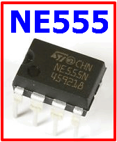
| Número de pieza | NE555 | |
| Descripción | SINGLE TIMER | |
| Fabricantes | Unisonic Technologies | |
| Logotipo | ||
 1. Bipolar Timer ( PDF ) Hay una vista previa y un enlace de descarga de NE555 (archivo pdf) en la parte inferior de esta página. Total 7 Páginas | ||
|
No Preview Available !
UNISONIC TECHNOLOGIES CO., LTD
NE555
LINEAR INTEGRATED CIRCUIT
SINGLE TIMER
DESCRIPTION
The UTC NE555 is a highly stable timer integrated circuit. It can
be operated in both Astable and Monostable mode. With monostable
operation, the time delay is precisely controlled by one external and
one capacitor. With a stable operation as an oscillator the frequency
and duty cycle are both accurately controlled with two external
resistors and one capacitor.
FEATURES
*High current driver capability (=200mA).
*Adjustable duty cycle.
*Timing from s to hours.
*Turn off time less than 2s.
*Operates in both astable and monostable modes.
■ ORDERING INFORMATION
Ordering Number
Lead Free
Halogen Free
NE555L-D08-T
NE555G-D08-T
- NE555G-S08-R
Package
DIP-8
SOP-8
Packing
Tube
Tape Reel
MARKING
DIP-8
SOP-8
www.unisonic.com.tw
Copyright © 2016 Unisonic Technologies Co., Ltd
1 of 7
QW-R106-001.G
1 page 
NE555
LINEAR INTEGRATED CIRCUIT
TYPICAL APPLICATION NOTES
The application circuit shows astable mode configuration.
Pin 6 (Threshold ) is tied to Pin 2 ( Trigger ) and Pin 4 ( reset ) is tied to VCC ( Pin 8 ). The external capacitor C1 of
Pin 6 and Pin 2 charges through RA, RB and dischages through RB only. In the internal circuit of UTC NE555N , one
input of the upper comparator is at voltage of 2/3VCC (R1=R2=R3),another input is connected to Pin 6.As soon as C1
is charging to higher than 2/3VCC, transistor Q1 is turned ON and discharge C1 to collector voltage of transistor Q1.
Therefore, the flip-flop circuit is reset and output is low. One input of lower comparator is at voltage of 1/3Vcc,
discharge transistor Q1 turn off and C1 charges through RA and RB. Therefore, the flip-flop circuit is set output high.
That is, when C1 charges through RA and RB, output is high and when C1 discharge through RB ,output is low.
The charge time(output is high) t1 is 0.693(RA+RB) C1 and the discharge time (output is low) T2 is 0.693 RB×C1.
In
VCC
VCC
-
-
1
3
2
3
VCC
VCC
=
0.693
T1=0.693×(RA+RB)×C1
Thus the total period time T is given by
T=T1+T2=0.693(RA+2RB)×C1.
T2=0.693×RB×C1
Then the frequency of astable mode is given by
1 1.44
f = T = (RA + 2RB)×C1
The duty cycle is given by
T2 RB
D.C.
T RA 2RB .
UNISONIC TECHNOLOGIES CO., LTD
www.unisonic.com.tw
5 of 7
QW-R106-001.G
5 Page | ||

| Páginas | Total 7 Páginas | |
| PDF Descargar | [ Datasheet NE555.PDF ] | |
Hoja de datos destacado
| Número de pieza | Descripción | Fabricantes |
| NE5500179A | SILICON POWER MOS FET | NEC |
| NE5500179A-T1 | SILICON POWER MOS FET | NEC |
| NE5510179A | 3.5V OPERATION SILICON RF POWER MOSFET | NEC |
| NE5510279A | 3.5V OPERATION SILICON RF POWER MOSFET | NEC |
| Número de pieza | Descripción | Fabricantes |
| SLA6805M | High Voltage 3 phase Motor Driver IC. |
Sanken |
| SDC1742 | 12- and 14-Bit Hybrid Synchro / Resolver-to-Digital Converters. |
Analog Devices |
|
DataSheet.es es una pagina web que funciona como un repositorio de manuales o hoja de datos de muchos de los productos más populares, |
| DataSheet.es | 2020 | Privacy Policy | Contacto | Buscar |