|
|
|
PDF STM8S005K6 Data sheet ( Hoja de datos )
| Número de pieza | STM8S005K6 | |
| Descripción | 8-bit MCU | |
| Fabricantes | STMicroelectronics | |
| Logotipo | ||
Hay una vista previa y un enlace de descarga de STM8S005K6 (archivo pdf) en la parte inferior de esta página. Total 30 Páginas | ||
|
No Preview Available !
STM8S005C6 STM8S005K6
Value line, 16 MHz STM8S 8-bit MCU, 32 Kbytes Flash, data
EEPROM, 10-bit ADC, timers, UART, SPI, I²C
Datasheet - production data
Features
Core
Max fCPU: 16 MHz
Advanced STM8 core with Harvard
architecture and 3-stage pipeline
Extended instruction set
Memories
Medium-density Flash/EEPROM
– Program memory: 32 Kbytes of Flash
memory; data retention 20 years at 55 °C
after 100 cycles
– Data memory: 128 bytes true data
EEPROM; endurance up to 100 k
write/erase cycles
RAM: 2 Kbytes
Clock, reset and supply management
2.95 V to 5.5 operating voltage
Flexible clock control, 4 master clock sources
– Low-power crystal resonator oscillator
– External clock input
– Internal, user-trimmable 16 MHz RC
– Internal low-power 128 kHz RC
Clock security system with clock monitor
Power management
– Low-power modes (wait, active-halt, halt)
– Switch-off peripheral clocks individually
– Permanently active, low-consumption
power-on and power-down reset
Interrupt management
Nested interrupt controller with 32 interrupts
Up to 37 external interrupts on 6 vectors
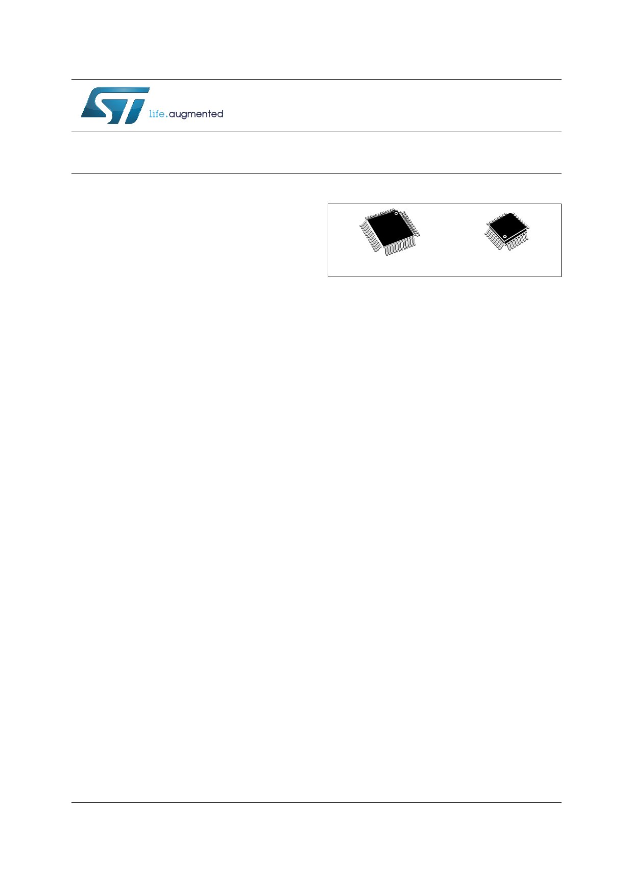
LQFP48
7 x 7mm
LQFP32
7 x 7mm
Timers
2x 16-bit general purpose timers, with 2+3
CAPCOM channels (IC, OC or PWM)
Advanced control timer: 16-bit, 4 CAPCOM
channels, 3 complementary outputs, dead-time
insertion and flexible synchronization
8-bit basic timer with 8-bit prescaler
Auto wakeup timer
Window and independent watchdog timers
Communications interfaces
UART with clock output for synchronous
operation, SmartCard, IrDA, LIN
SPI interface up to 8 Mbit/s
I2C interface up to 400 Kbit/s
Analog to digital converter (ADC)
10-bit ADC, ± 1 LSB ADC with up to 10
multiplexed channels, scan mode and analog
watchdog
I/Os
Up to 38 I/Os on a 48-pin package including 16
high-sink outputs
Highly robust I/O design, immune against
current injection
Development support
Embedded single-wire interface module
(SWIM) for fast on-chip programming and non-
intrusive debugging
March 2015
This is information on a product in full production.
DocID022186 Rev 4
1/97
www.st.com
1 page 
STM8S005C6 STM8S005K6
List of tables
List of tables
Table 1.
Table 2.
Table 3.
Table 4.
Table 5.
Table 6.
Table 7.
Table 8.
Table 9.
Table 10.
Table 11.
Table 12.
Table 13.
Table 14.
Table 15.
Table 16.
Table 17.
Table 18.
Table 19.
Table 20.
Table 21.
Table 22.
Table 23.
Table 24.
Table 25.
Table 26.
Table 27.
Table 28.
Table 29.
Table 30.
Table 31.
Table 32.
Table 33.
Table 34.
Table 35.
Table 36.
Table 37.
Table 38.
Table 39.
Table 40.
Table 41.
Table 42.
Table 43.
Table 44.
Table 45.
Table 46.
Table 47.
Table 48.
STM8S005C6/K6 value line features . . . . . . . . . . . . . . . . . . . . . . . . . . . . . . . . . . . . . . . . . 10
Peripheral clock gating bit assignments in CLK_PCKENR1/2 registers . . . . . . . . . . . . . . . 15
TIM timer features. . . . . . . . . . . . . . . . . . . . . . . . . . . . . . . . . . . . . . . . . . . . . . . . . . . . . . . . 18
Legend/abbreviations for STM8S005C6/K6 pin descriptions table . . . . . . . . . . . . . . . . . . 22
STM8S005C6 and STM8S005K6 pin descriptions . . . . . . . . . . . . . . . . . . . . . . . . . . . . . . . 23
Flash, Data EEPROM and RAM boundary addresses . . . . . . . . . . . . . . . . . . . . . . . . . . . . 27
I/O port hardware register map . . . . . . . . . . . . . . . . . . . . . . . . . . . . . . . . . . . . . . . . . . . . . . 27
General hardware register map . . . . . . . . . . . . . . . . . . . . . . . . . . . . . . . . . . . . . . . . . . . . . 29
CPU/SWIM/debug module/interrupt controller registers . . . . . . . . . . . . . . . . . . . . . . . . . . . 35
Interrupt mapping . . . . . . . . . . . . . . . . . . . . . . . . . . . . . . . . . . . . . . . . . . . . . . . . . . . . . . . . 37
Option bytes . . . . . . . . . . . . . . . . . . . . . . . . . . . . . . . . . . . . . . . . . . . . . . . . . . . . . . . . . . . . 38
Option byte description . . . . . . . . . . . . . . . . . . . . . . . . . . . . . . . . . . . . . . . . . . . . . . . . . . . . 39
Description of alternate function remapping bits [7:0] of OPT2 . . . . . . . . . . . . . . . . . . . . . 41
Voltage characteristics . . . . . . . . . . . . . . . . . . . . . . . . . . . . . . . . . . . . . . . . . . . . . . . . . . . . 44
Current characteristics . . . . . . . . . . . . . . . . . . . . . . . . . . . . . . . . . . . . . . . . . . . . . . . . . . . . 45
Thermal characteristics. . . . . . . . . . . . . . . . . . . . . . . . . . . . . . . . . . . . . . . . . . . . . . . . . . . . 45
General operating conditions . . . . . . . . . . . . . . . . . . . . . . . . . . . . . . . . . . . . . . . . . . . . . . . 46
Operating conditions at power-up/power-down . . . . . . . . . . . . . . . . . . . . . . . . . . . . . . . . . 47
Total current consumption with code execution in run mode at VDD = 5 V . . . . . . . . . . . . 49
Total current consumption with code execution in run mode at VDD = 3.3 V . . . . . . . . . . . 50
Total current consumption in wait mode at VDD = 5 V . . . . . . . . . . . . . . . . . . . . . . . . . . . . 51
Total current consumption in wait mode at VDD = 3.3 V . . . . . . . . . . . . . . . . . . . . . . . . . . 51
Total current consumption in active halt mode at VDD = 5 V, TA -40 to 85° C . . . . . . . . . . 52
Total current consumption in active halt mode at VDD = 3.3 V . . . . . . . . . . . . . . . . . . . . . 52
Total current consumption in halt mode at VDD = 5 V, TA -40 to 85° C . . . . . . . . . . . . . . . 53
Total current consumption in halt mode at VDD = 3.3 V . . . . . . . . . . . . . . . . . . . . . . . . . . . 53
Wakeup times . . . . . . . . . . . . . . . . . . . . . . . . . . . . . . . . . . . . . . . . . . . . . . . . . . . . . . . . . . . 53
Total current consumption and timing in forced reset state . . . . . . . . . . . . . . . . . . . . . . . . 54
Peripheral current consumption . . . . . . . . . . . . . . . . . . . . . . . . . . . . . . . . . . . . . . . . . . . . . 54
HSE user external clock characteristics . . . . . . . . . . . . . . . . . . . . . . . . . . . . . . . . . . . . . . . 58
HSE oscillator characteristics . . . . . . . . . . . . . . . . . . . . . . . . . . . . . . . . . . . . . . . . . . . . . . . 59
HSI oscillator characteristics. . . . . . . . . . . . . . . . . . . . . . . . . . . . . . . . . . . . . . . . . . . . . . . . 60
LSI oscillator characteristics . . . . . . . . . . . . . . . . . . . . . . . . . . . . . . . . . . . . . . . . . . . . . . . . 61
RAM and hardware registers . . . . . . . . . . . . . . . . . . . . . . . . . . . . . . . . . . . . . . . . . . . . . . . 62
Flash program memory/data EEPROM memory . . . . . . . . . . . . . . . . . . . . . . . . . . . . . . . . 62
I/O static characteristics . . . . . . . . . . . . . . . . . . . . . . . . . . . . . . . . . . . . . . . . . . . . . . . . . . . 63
Output driving current (standard ports) . . . . . . . . . . . . . . . . . . . . . . . . . . . . . . . . . . . . . . . . 65
Output driving current (true open drain ports). . . . . . . . . . . . . . . . . . . . . . . . . . . . . . . . . . . 65
Output driving current (high sink ports). . . . . . . . . . . . . . . . . . . . . . . . . . . . . . . . . . . . . . . . 66
NRST pin characteristics . . . . . . . . . . . . . . . . . . . . . . . . . . . . . . . . . . . . . . . . . . . . . . . . . . 72
SPI characteristics . . . . . . . . . . . . . . . . . . . . . . . . . . . . . . . . . . . . . . . . . . . . . . . . . . . . . . . 74
I2C characteristics. . . . . . . . . . . . . . . . . . . . . . . . . . . . . . . . . . . . . . . . . . . . . . . . . . . . . . . . 77
ADC characteristics . . . . . . . . . . . . . . . . . . . . . . . . . . . . . . . . . . . . . . . . . . . . . . . . . . . . . . 79
ADC accuracy with RAIN < 10 k, VDDA = 5 V. . . . . . . . . . . . . . . . . . . . . . . . . . . . . . . . . . 80
ADC accuracy with RAIN < 10 kRAIN, VDDA = 3.3 V. . . . . . . . . . . . . . . . . . . . . . . . . . . . . 80
EMS data . . . . . . . . . . . . . . . . . . . . . . . . . . . . . . . . . . . . . . . . . . . . . . . . . . . . . . . . . . . . . . 82
EMI data . . . . . . . . . . . . . . . . . . . . . . . . . . . . . . . . . . . . . . . . . . . . . . . . . . . . . . . . . . . . . . 83
ESD absolute maximum ratings . . . . . . . . . . . . . . . . . . . . . . . . . . . . . . . . . . . . . . . . . . . . . 83
DocID022186 Rev 4
5/97
6
5 Page 
STM8S005C6 STM8S005K6
3 Block diagram
Block diagram
Figure 1. STM8S005C6/K6 value line block diagram
Reset
Single wire
debug interf.
Master/slave
autosynchro
LIN master
SPI emul.
400 Kbit/s
8 Mbit/s
up to 10
channels
1/2/4 kHz beep
Reset block
Reset
POR
BOR
Clock controller
Detector
XTAL 1-16 MHz
RC int. 16 MHz
RC int. 128 kHz
Clock to peripherals and core
STM8 core
Debug/SWIM
UART2
I2C
SPI
ADC1
Beeper
Window WDG
Independent WDG
32 Kbytes high
density program Flash
128 bytes
data EEPROM
2 Kbytes RAM
Boot ROM
16-bit advanced control
timer (TIM1)
16-bit general purpose
timers (TIM2, TIM3)
8-bit basic timer
(TIM4)
Up to
4 CAPCOM
channels
+ 3 complementary
outputs
Up to
5 CAPCOM
channels
AWU timer
DocID022186 Rev 4
11/97
25
11 Page | ||
| Páginas | Total 30 Páginas | |
| PDF Descargar | [ Datasheet STM8S005K6.PDF ] | |
Hoja de datos destacado
| Número de pieza | Descripción | Fabricantes |
| STM8S005K6 | 8-bit MCU | STMicroelectronics |
| Número de pieza | Descripción | Fabricantes |
| SLA6805M | High Voltage 3 phase Motor Driver IC. |
Sanken |
| SDC1742 | 12- and 14-Bit Hybrid Synchro / Resolver-to-Digital Converters. |
Analog Devices |
|
DataSheet.es es una pagina web que funciona como un repositorio de manuales o hoja de datos de muchos de los productos más populares, |
| DataSheet.es | 2020 | Privacy Policy | Contacto | Buscar |