|
|
|
PDF PCA9535E Data sheet ( Hoja de datos )
| Número de pieza | PCA9535E | |
| Descripción | 16-bit Low-Power I/O Expander | |
| Fabricantes | ON Semiconductor | |
| Logotipo | ||
Hay una vista previa y un enlace de descarga de PCA9535E (archivo pdf) en la parte inferior de esta página. Total 20 Páginas | ||
|
No Preview Available !
PCA9535E, PCA9535EC
16-bit Low-Power I/O
Expander for I2C Bus with
Interrupt
The PCA9535E and PCA9535EC devices provide 16 bits of
General Purpose parallel Input / Output (GPIO) expansion through the
I2C−bus / SMBus.
www.onsemi.com
The PCA9535E and PCA9535EC consist of two 8−bit
MARKING
Configuration (Input or Output selection); Input, Output and Polarity
DIAGRAMS
Inversion (active−HIGH or active−LOW operation) registers. At
power on, all I/Os default to inputs. Each I/O may be configured as
either input or output by writing to its corresponding I/O configuration
bit. The data for each Input or Output is kept in its corresponding Input
or Output register. The Polarity Inversion register may be used to
invert the polarity if the read register. All registers can be read by the
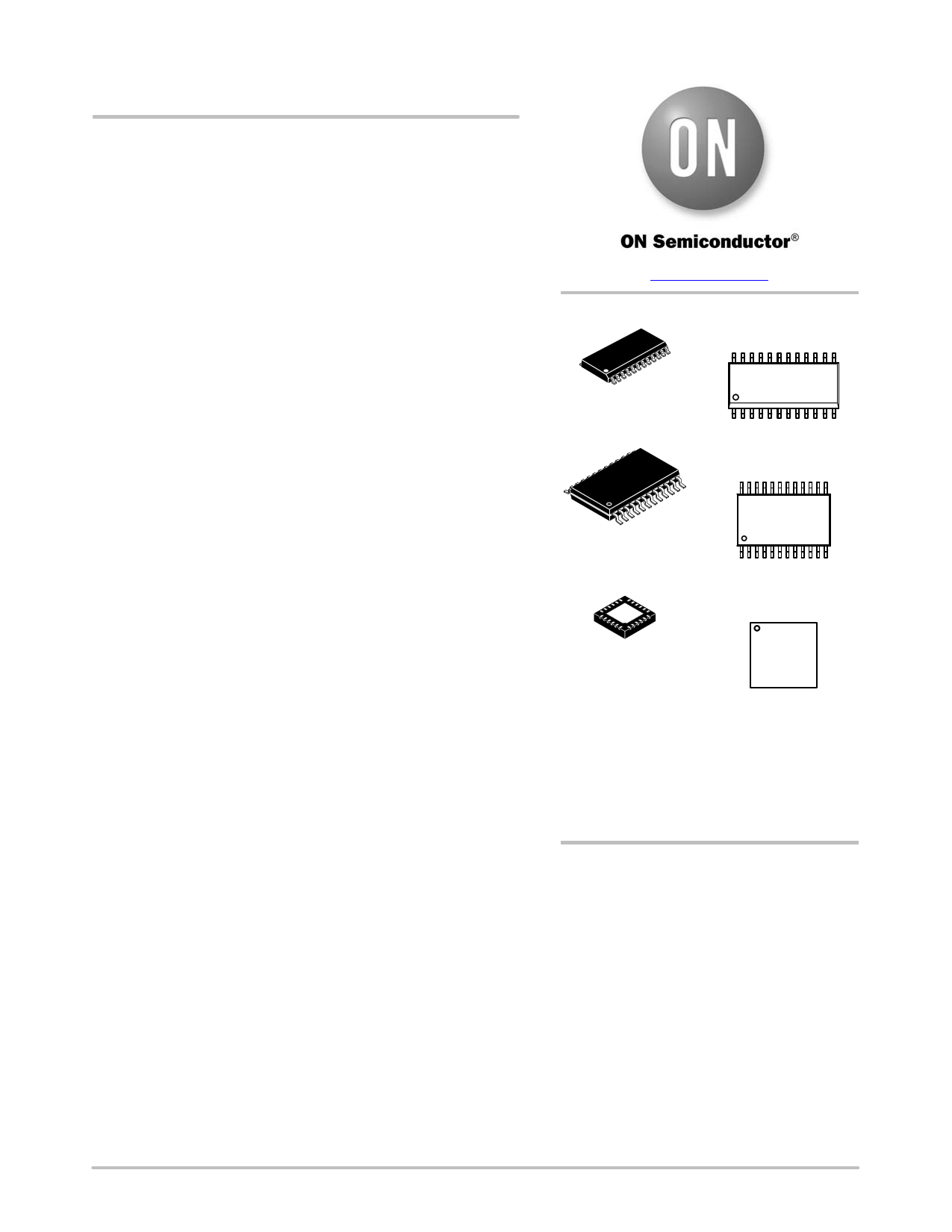
SOIC−24
DW SUFFIX
CASE 751E
PCA9535E(C)
AWLYYWWG
system master.
The PCA9535E, identical to the PCA9655E but with the internal
I/O pull−up resistors removed, has greatly reduced power
consumption when the I/Os are held LOW.
The PCA9535EC is identical to the PCA9535E but with
high−impedance open−drain outputs at all the I/O pins.
The PCA9535E and PCA9535EC provide an open−drain interrupt
output which is activated when any input state differs from its
TSSOP−24
DT SUFFIX
CASE 948H
PCA95
35E(C)G
ALYW
corresponding input port register state. The interrupt output is used to
indicate to the system master that an input state has changed. The
power−on reset sets the registers to their default values and initializes
the device state machine.
Three hardware pins (AD0, AD1, AD2) are used to configure the
I2C−bus slave address of the device. The I2C−bus slave addresses of
1
WQFN24
MT SUFFIX
CASE 485BG
PCA
9535E(C)
ALYWG
G
the PCA9535E and PCA9535EC are the same as the PCA9655E. This
allows up to 64 of these devices in any combination to share the same
I2C−bus/SMBus.
XXXX
A
WL, L
YY, Y
= Specific Device Code
= Assembly Location
= Wafer Lot
= Year
Features
• VDD Operating Range: 1.65 V to 5.5 V
• SDA Sink Capability: 30 mA
WW, W = Work Week
G or G = Pb−Free Package
(Note: Microdot may be in either location)
• 5.5 V Tolerant I/Os
• Polarity Inversion Register
• Active LOW Interrupt Output
ORDERING INFORMATION
See detailed ordering and shipping information in the package
dimensions section on page 17 of this data sheet.
• Low Standby Current
• Noise Filter on SCL/SDA Inputs
• ESD Performance: 3000 V Human Body Model, 400 V
• No Glitch on Power−up
• Internal Power−on Reset
Machine Model
• NLV Prefix for Automotive and Other Applications
• 64 Programmable Slave Addresses using Three
Address Pins
• 16 I/O Pins which Default to 16 Inputs
• I2C SCL Clock Frequencies Supported:
Requiring Unique Site and Control Change
Requirements; AEC−Q100 Qualified and PPAP
Capable
• These are Pb−Free Devices
Standard Mode: 100 kHz
Fast Mode: 400 kHz
Fast Mode +: 1 MHz
© Semiconductor Components Industries, LLC, 2015
October, 2015 − Rev. 6
1
Publication Order Number:
PCA9535E/D
1 page 
PCA9535E, PCA9535EC
Table 4. DC ELECTRICAL CHARACTERISTICS VDD = 1.65 V to 5.5 V, unless otherwise specified.
TA = −555C to +1255C
Symbol
Parameter
Conditions
Min Typ Max Unit
SUPPLIES
ISTB Standby Current (Note 6)
VPOR
Power−On Reset Voltage (Note 7)
INPUT SCL; INPUT / OUTPUT SDA
VIH High−Level Input Voltage
VIL Low−Level Input Voltage
IOL Low−Level Output Current
IL
CI
I/Os
Leakage Current
Input Capacitance
Standby mode; no load;
VI = 0 V; fSCL = 0 Hz; I/O = inputs
VI = VDD; fSCL = 0 Hz; I/O = inputs
VOL = 0.4 V; VDD < 2.3 V
VOL = 0.4 V; VDD w 2.3 V
VI = VDD or 0 V
VI = 0 V
mA
39 100
39 100
1.5 1.65
V
0.7 x VDD
10
20
0.3 x VDD
V
V
mA
$1 mA
4.6 6 pF
VIH High−Level Input Voltage
VIL Low−Level Input Voltage
IOL Low−Level Output Current
(Note 8)
IOL(tot)
Total Low−Level Output Current
(Note 8)
VOL = 0.5 V; VDD = 1.65 V
VOL = 0.5 V; VDD = 2.3 V
VOL = 0.5 V; VDD = 3.0 V
VOL = 0.5 V; VDD = 4.5 V
VOL = 0.5 V; VDD = 4.5 V
0.7 x VDD
V
0.3 x VDD
V
8 20
mA
12 28
17 35
25 42
400 mA
VOH High−Level Output Voltage
(PCA9535E Only)
IL Input Leakage Current
CI/O Input / Output Capacitance
(Note 9)
IOH = −3 mA; VDD = 1.65 V
IOH = −4 mA; VDD = 1.65 V
IOH = −8 mA; VDD = 2.3 V
IOH = −10 mA; VDD = 2.3 V
IOH = −8 mA; VDD = 3.0 V
IOH = −10 mA; VDD = 3.0 V
IOH = −8 mA; VDD = 4.5 V
IOH = −10 mA; VDD = 4.5 V
VDD = 5.5 V; VI = VDD or 0 V
1.2 V
1.1
1.8
1.7
2.6
2.5
4.1
4.0
$1 mA
3.7 5 pF
INTERRUPT (INT)
IOL Low−Level Output Current
CO Output Capacitance
VOL = 0.4 V
6 mA
2.1 5 pF
INPUTS AD0, AD1, AD2
VIH High−Level Input Voltage
VIL Low−Level Input Voltage
IL Leakage Current
CI Input Capacitance
VI = VDD or 0 V
0.7 x VDD
0.3 x VDD
$1
V
V
mA
2.4 5 pF
6. The device is in standby mode after an I2C stop command.
7. The power−on reset circuit resets the I2C bus logic with VDD < VPOR and set all I/Os to logic 1 upon power−up. Thereafter, VDD must
be lower than 0.2 V to reset the part.
8. Each bit must be limited to a maximum of 25 mA and the total package limited to 400 mA due to internal busing limits.
9. The value is not tested, but verified on sampling basis.
www.onsemi.com
5
5 Page 
PCA9535E, PCA9535EC
BUS TRANSACTIONS
Writing to the Port Registers
To transmit data to the PCA9535E/PCA9535EC, the bus
master must first send the device address with the least
significant bit set to logic 0 (see Figure 5 “PCA9535E and
PCA9535EC device address”). The command byte is sent
after the address and determines which registers will receive
the data following the command byte.
There are eight registers within the
PCA9535E/PCA9535EC. These registers are configured to
operate as four register pairs: Input Ports, Output Ports,
Polarity Inversion Ports, and Configuration Ports. Data
bytes are sent alternately to each register in a register pair
(see Figures 6 and 7). For example, if one byte is sent to
Output Port 1 (register 3), then the next byte will be stored
in Output Port 0 (register 2). There is no limitation on the
number of data bytes sent in one write transmission. In this
way, each 8−bit register may be updated independently of
the other registers.
SCL 1 2 3 4 5 6 7 8 9
slave address
command byte
SDA S A6 A5 A4 A3 A2 A1 A0 0 A 0 0 0 0 0 0 1 0 A 0.7
data to port 0
DATA 0
0.0 A 1.7
data to port 1
DATA 1
1.0 A P
START condition
R/W acknowledge
from slave
acknowledge
from slave
acknowledge
from slave
STOP
condition
write to port
data out
from port 0
data out
from port 1
tv(Q)
Figure 6. Write to Output Port Registers
tv(Q)
DATA VALID
SCL 1 2 3 4 5 6 7 8 9
slave address
SDA S A6 A5 A4 A3 A2 A1 A0 0 A 0
command byte
MSB
0 0 0 0 1 1 0A
data to register
DATA 0
LSB MSB
A
data to register
DATA 1
LSB
AP
START condition
R/W acknowledge
from slave
acknowledge
from slave
Figure 7. Write to Configuration Registers
acknowledge
from slave
STOP
condition
Reading the Port Registers
To read data from the PCA9535E/PCA9535EC, the bus
master must first send the PCA9535E/PCA9535EC address
with the least significant bit set to logic 0 (see Figure 5
“PCA9535E and PCA9535EC device address”). The
command byte is sent after the address and determines
which register will be accessed.
After a restart, the device address must be sent again, but
this time, the least significant bit is set to logic 1. Data from
the register defined by the command byte will then be sent
by the PCA9535E/PCA9535EC (see Figures 8, 9 and 10).
Data is clocked into the register on the falling edge of the
acknowledge clock pulse. After the first byte is read,
additional bytes may be read but with data alternately
coming from each register in the pair. For example, if you
read Input Port 1, then the next byte read would be
Input Port 0. There is no limitation on the number of data
bytes received in one read transmission but the bus master
must not acknowledge the data for the final byte received.
www.onsemi.com
11
11 Page | ||
| Páginas | Total 20 Páginas | |
| PDF Descargar | [ Datasheet PCA9535E.PDF ] | |
Hoja de datos destacado
| Número de pieza | Descripción | Fabricantes |
| PCA9535 | 16-bit I2C and SMBus/ low power I/O port with interrupt | NXP Semiconductors |
| PCA9535 | PCA9535 Remote 16-Bit I2C and SMBus Low-Power I/O Expander (Rev. J) | Texas Instruments |
| PCA9535BS | 16-bit I2C and SMBus/ low power I/O port with interrupt | NXP Semiconductors |
| PCA9535D | 16-bit I2C and SMBus/ low power I/O port with interrupt | NXP Semiconductors |
| Número de pieza | Descripción | Fabricantes |
| SLA6805M | High Voltage 3 phase Motor Driver IC. |
Sanken |
| SDC1742 | 12- and 14-Bit Hybrid Synchro / Resolver-to-Digital Converters. |
Analog Devices |
|
DataSheet.es es una pagina web que funciona como un repositorio de manuales o hoja de datos de muchos de los productos más populares, |
| DataSheet.es | 2020 | Privacy Policy | Contacto | Buscar |