|
|
|
PDF SKY73100-11 Data sheet ( Hoja de datos )
| Número de pieza | SKY73100-11 | |
| Descripción | 865-960 MHz High Performance VCO/Synthesizer | |
| Fabricantes | Skyworks Solutions | |
| Logotipo | ||
Hay una vista previa y un enlace de descarga de SKY73100-11 (archivo pdf) en la parte inferior de esta página. Total 21 Páginas | ||
|
No Preview Available !
DATA SHEET
SKY73100-11: 865-960 MHz High Performance
VCO/Synthesizer
Applications
• 2G, 2.5G, and 3G base station transceivers:
− GSM, EDGE, CDMA, WCDMA
• General purpose RF systems
Features
• Frequency operation range: 865 to 960 MHz
• Process-tolerant compensation for VCO
• 24-bit Σ∆ fractional-N synthesizer
• Ultra-fine frequency resolution of 0.001 ppm
• Flexible reference frequency selection
• Three-wire serial interface up to 20 MHz clock frequency
• Integrated PLL supply regulation for spur isolation
• MCM (38-pin, 9 x 12 mm) Pb-free free (MSL3, 260 °C per
JEDEC J-STD-020) SMT package
Skyworks offers lead (Pb)-free, RoHS (Restriction of
Hazardous Substances) compliant packaging.
Description
Skyworks SKY73100-11 Voltage-Controlled Oscillator
(VCO)/Synthesizer is a fully integrated, high performance signal
source for high dynamic range transceivers. The device provides
ultra-fine frequency resolution, fast switching speed, and low
phase noise performance for 2G, 2.5G, and 3G base station
transceivers.
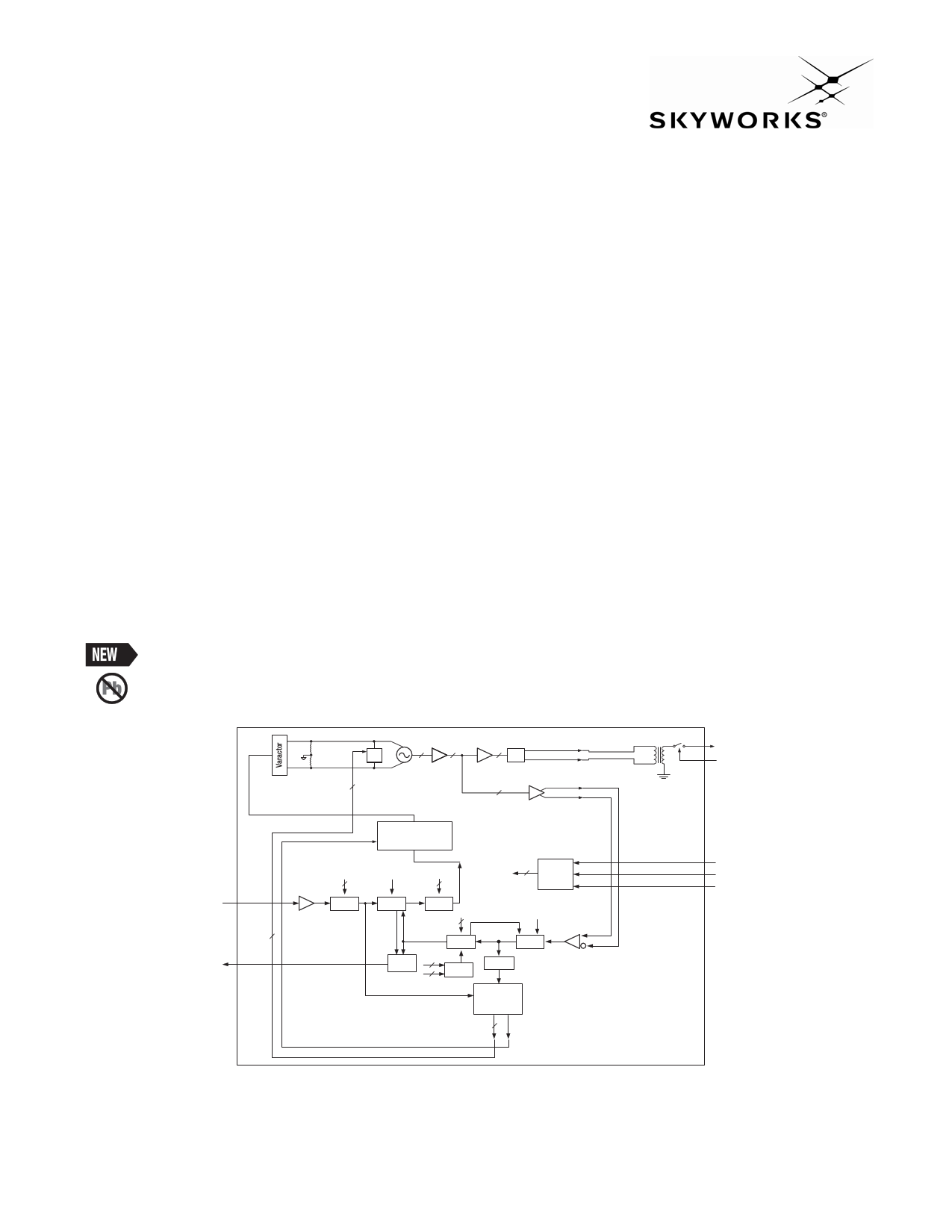
The SKY73100-11 VCO/Synthesizer is a key building block for
high-performance radio system designs that require low power
and a fine step size. Reference clock generators with an output
frequency up to 52 MHz can be used with the SKY73100-11. A
functional block diagram is shown in Figure 1. As indicated in this
diagram, the reference frequency is divided down by 1, 2, 4, or 8
in the R1 divider, depending on the value of the reference divisor
input (R1). Refer to the Reference Input Divider section (page 10)
for more information.
The SKY73100-11 VCO/Synthesizer is provided in a compact, 38-
pin Multi-Chip Module (MCM). The device package and pinout are
shown in Figure 2. Signal pin assignments and functional pin
descriptions are provided in Table 1.
Vtune
FREF
7
LD
Lr VCO Out +
Lr
Cal
22
Buffer
2
VCO Out –
7
cap [6:0]
Flag
Vtune
PLL
Low Pass Filter
SR Out +
2 SR Out –
R1
R1
Divider
SP1 SC1 CPO RF
RF RF Charge
PFD Pump
N
3-Wire
Serial
Interface
PS
Mux
(LD/Test)
FN
ME
N
Divider
P/P+1
Prescaler
ΔΣ
Modulator
Divide-by-2
Digital
Coarse
Calibration
cap [6:0]
7
Calibration
Complete
RFIN
RFINB
Z = 1:4
RF Output
SW_EN
CLK
LE
DAT
Figure 1. SKY73100-11 Functional Block Diagram
S1040
Skyworks Solutions, Inc. • Phone [781] 376-3000 • Fax [781] 376-3100 • [email protected] • www.skyworksinc.com
200361B • Skyworks Proprietary and Confidential Information • Products and Product Information are Subject to Change Without Notice • April 15, 2009
1
1 page 
DATA SHEET • SKY73100-11 VCO/SYNTHESIZER
Table 4. Load Register Word 0 (Programs the Operation Mode Register) (1 of 2)
Parameter
Function
State Description
wd_0, wd_1
cp_output
cp_delay
pd_polar
cp_tristate
rsvd
sd_sel
nr_sel
pll_en
ref_bw_sel
Address bits [1:0]. Must be set to 00b (see
Table 3)
Charge pump setting [4:2]
Charge pump delay [6:5]
Polarity of phase detector [7]
Tri-state selection for the transmit PLL
charge pump output [8]
Reserved [9]
Internal operating voltage control bit for Σ∆
synthesizer [10]
Note: this bit needs to be programmed
together with bits [11] and [12].
Internal operating voltage control bit for N-
counter and R1 divider [11]
See sd_sel parameter (bit [10])
Internal operating voltage control bit for PLL
[12]
See sd_sel parameter (bit [10])
Reference buffer bandwidth [14:13]
Bits [4:2]:
0 0 0 = 200 µA
0 0 1 = 400 µA
0 1 0 = 600 µA
0 1 1 = 800 µA
1 0 0 = 1000 µA
1 0 1 = 1200 µA
1 1 0 = 1400 µA
1 1 1 = 1600 µA
Bits [6:5]:
0 0 = 2 nsec
0 1 = 4 nsec
1 0 = 7 nsec
1 1 = 9 nsec
NOTE: this device is fixed at 2 nsec.
Bit [7]:
0 = Negative
1 = Positive
NOTE: this device is fixed at negative polarity.
Bit [8]:
0 = Charge pump in normal functional mode
1 = Charge pump disabled/tri-stated
Reserved
Bit [12] Bit [11] Bit [10]: N-Cntr/R1-Divider ΣΔ Mod
Voltage
Voltage
0X
10
10
11
11
X=
0=
1=
0=
1=
0V
1.8 V
1.8 V
2.4 V
2.4 V
0V
1.8 V
2.4 V
1.8 V
2.4 V
This bit needs to be programmed together with bits [10] and [12].
This bit needs to be programmed together with bits [10] and [11].
Bits [14:13]:
0 0 = 20 MHz
0 1 = 30 MHz
1 0 = 40 MHz
1 1 = 50 MHz
Recommended
Operational Value
(Binary)
00
Application
dependent
00
0
0
0
100
–
–
11
Skyworks Solutions, Inc. • Phone [781] 376-3000 • Fax [781] 376-3100 • [email protected] • www.skyworksinc.com
200361B • Skyworks Proprietary and Confidential Information • Products and Product Information are Subject to Change Without Notice • April 15, 2009
5
5 Page 
The value of ME is equal to the binary representation of the
integer part of 223 × MEactual, or:
ME = D14 × 214 + D13 × 213 + D12 × 212 + . . .D0
Example :
A desired synthesizer frequency of 960 MHz is required using a
crystal frequency of 52 MHz and an 8/9 prescaler. Since the
maximum internal reference frequency is 25 MHz, the crystal
frequency needs to be divided; a reference divider ratio of 8 is
used for this example.
Restating Equation (2) as a function of DTotal:
DTotal = (960 × 8)/52 = 147.692307692308
Where: RF = 960
R1 = 8
FREF = 52
Determine Nactual by subtracting 3.5 from DTotal and removing the
fractional portion:
DTotal – 3.5 = 144.192307692308
Using Equation (3):
Nactual = 144 = Mactual × P + Aactual
where: Mactual = 18
P=8
Aactual = 0
M = Mactual = 18 = 010010b (the six MSBs)
A = Aactual = 0 = 0000b (the four LSBs)
N = M × 24 + A = 0100100000b (the value programmed)
Multiply the fractional portion that was removed in the previous
step by 256 and remove the fractional portion of the result to
determine FN:
0.192307692308 × 256 = 49.230769230848
FN = 49 = 00110001b (the value programmed)
Divide FN by 256 to determine the actual fractional part, FNactual:
FNactual = 49/256 = 0.19140625
Subtract this result from the fractional portion of DTotal – 3.5 to
determine the actual fractional modulus extender, MEactual:
MEactual = (DTotal – 3.5 – Nactual) – FNactual
= 0.192307692308 – 0.19140625
= 0.00090144230767919
DATA SHEET • SKY73100-11 VCO/SYNTHESIZER
Multiply this result by 8388608 (the 23-bit ∆Σ modulator value,
223) and remove the fractional portion to determine the value of
ME:
0.00090144230767919 × 8388608 = 7561.84615373611
ME = 7561 = 001110110001001b (the value programmed). Refer
to Tables 6 and 7 for the location of the resulting bits in the ME
parameter.
Package and Handling Information
Since the device package is sensitive to moisture absorption, it is
baked and vacuum packed before shipping. Instructions on the
shipping container label regarding exposure to moisture after the
container seal is broken must be followed. Otherwise, problems
related to moisture absorption may occur when the part is
subjected to high temperature during solder assembly.
The SKY73100-11 is rated to Moisture Sensitivity Level 3 (MSL3)
at 260 °C. It can be used for lead or lead-free soldering. For
additional information, refer to Skyworks Application Note, PCB
Design and SMT Assembly/Rework Guidelines for MCM-L
Packages, document number 101752.
Care must be taken when attaching this product, whether it is
done manually or in a production solder reflow environment.
Production quantities of this product are shipped in a standard
tape and reel format. For packaging details, refer to the Skyworks
Application Note, Tape and Reel, document number 101568.
Circuit Design Considerations
The following design considerations are general in nature and
must be followed regardless of final use or configuration
1. Paths to ground should be made as short and as low
impedance as possible.
2. The ground pad of the SKY73100-11 provides critical
electrical grounding requirements. Design the connection to
the ground pad to provide the best electrical connection to the
circuit board. Multiple vias to the grounding layer are
recommended to connect the top layer ground area to the
main ground layer.
3. Skyworks recommends including external bypass capacitors
on the VDD voltage input (pin 37) of the device. These
capacitors should be placed as close as possible to the VDD
input pin.
4. A 50 Ω impedance trace is needed for the RF_OUT (pin 10)
line.
Skyworks Solutions, Inc. • Phone [781] 376-3000 • Fax [781] 376-3100 • [email protected] • www.skyworksinc.com
200361B • Skyworks Proprietary and Confidential Information • Products and Product Information are Subject to Change Without Notice • April 15, 2009
11
11 Page | ||
| Páginas | Total 21 Páginas | |
| PDF Descargar | [ Datasheet SKY73100-11.PDF ] | |
Hoja de datos destacado
| Número de pieza | Descripción | Fabricantes |
| SKY73100-11 | 865-960 MHz High Performance VCO/Synthesizer | Skyworks Solutions |
| Número de pieza | Descripción | Fabricantes |
| SLA6805M | High Voltage 3 phase Motor Driver IC. |
Sanken |
| SDC1742 | 12- and 14-Bit Hybrid Synchro / Resolver-to-Digital Converters. |
Analog Devices |
|
DataSheet.es es una pagina web que funciona como un repositorio de manuales o hoja de datos de muchos de los productos más populares, |
| DataSheet.es | 2020 | Privacy Policy | Contacto | Buscar |