|
|
|
PDF D5N40 Data sheet ( Hoja de datos )
| Número de pieza | D5N40 | |
| Descripción | HFD5N40 | |
| Fabricantes | SemiHow | |
| Logotipo | ||
 1. Transistor ( PDF Datasheet ) Hay una vista previa y un enlace de descarga de D5N40 (archivo pdf) en la parte inferior de esta página. Total 8 Páginas | ||
|
No Preview Available !
July 2005
HFD5N40 / HFU5N40
400V N-Channel MOSFET
BVDSS = 400 V
RDS(on) typ = 1.27 Ω
ID = 3.4 A
FEATURES
Originative New Design
Superior Avalanche Rugged Technology
Robust Gate Oxide Technology
Very Low Intrinsic Capacitances
Excellent Switching Characteristics
Unrivalled Gate Charge : 13 nC (Typ.)
Extended Safe Operating Area
Lower RDS(ON) : 1.27 Ω (Typ.) @VGS=10V
100% Avalanche Tested
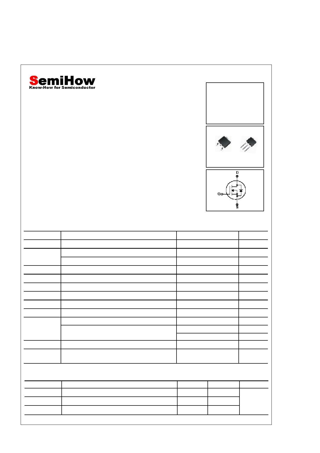
D-PAK I-PAK
2
1
3
HFD5N40
1
2
3
HFU5N40
1.Gate 2. Drain 3. Source
Absolute Maximum Ratings TC=25℃ unless otherwise specified
Symbol
Parameter
Value
VDSS
ID
IDM
VGS
EAS
IAR
EAR
dv/dt
Drain-Source Voltage
Drain Current
Drain Current
Drain Current
– Continuous (TC = 25℃)
– Continuous (TC = 100℃)
– Pulsed
(Note 1)
Gate-Source Voltage
Single Pulsed Avalanche Energy
(Note 2)
Avalanche Current
(Note 1)
Repetitive Avalanche Energy
(Note 1)
Peak Diode Recovery dv/dt
(Note 3)
400
3.4
2.15
13.6
±30
510
3.4
4.5
4.5
PD
TJ, TSTG
TL
Power Dissipation (TA = 25℃)
Power Dissipation (TC = 25℃)
- Derate above 25℃
Operating and Storage Temperature Range
Maximum lead temperature for soldering purposes,
1/8” from case for 5 seconds
2.5
45
0.36
-55 to +150
300
Units
V
A
A
A
V
mJ
A
mJ
V/ns
W
W
W/℃
℃
℃
Thermal Resistance Characteristics
Symbol
Parameter
RθJC Junction-to-Case
RθJA Junction-to-Ambient*
RθJA Junction-to-Ambient
* When mounted on the minimum pad size recommended (PCB Mount)
Typ.
--
--
--
Max.
2.78
50
110
Units
℃/W
◎ SEMIHOW REV.A0,July 2005
1 page 
Fig 12. Gate Charge Test Circuit & Waveform
Same Type
50KΩ
as DUT
12V 200nF
300nF
VGS
10V
Qg
VGS
VDS
Qgs Qgd
DUT
3mA
Charge
10V
10V
Fig 13. Resistive Switching Test Circuit & Waveforms
VDS
RG
RL
VDD
( 0.5 rated VDS )
DUT
VDS
90%
10%
Vin
td(on)
tr
t on
td(off)
tf
t off
Fig 14. Unclamped Inductive Switching Test Circuit & Waveforms
VDS
ID
RG
L
VDD
EAS =
--1--
2
LL IAS2
BVDSS
--------------------
BVDSS -- VDD
BVDSS
IAS
ID (t)
DUT
VDD
VDS (t)
t p Time
◎ SEMIHOW REV.A0,July 2005
5 Page | ||
| Páginas | Total 8 Páginas | |
| PDF Descargar | [ Datasheet D5N40.PDF ] | |
Hoja de datos destacado
| Número de pieza | Descripción | Fabricantes |
| D5N40 | HFD5N40 | SemiHow |
| Número de pieza | Descripción | Fabricantes |
| SLA6805M | High Voltage 3 phase Motor Driver IC. |
Sanken |
| SDC1742 | 12- and 14-Bit Hybrid Synchro / Resolver-to-Digital Converters. |
Analog Devices |
|
DataSheet.es es una pagina web que funciona como un repositorio de manuales o hoja de datos de muchos de los productos más populares, |
| DataSheet.es | 2020 | Privacy Policy | Contacto | Buscar |