|
|
|
PDF CH455 Data sheet ( Hoja de datos )
| Número de pieza | CH455 | |
| Descripción | LED drive and keyboard control chip | |
| Fabricantes | ETC | |
| Logotipo | ||
Hay una vista previa y un enlace de descarga de CH455 (archivo pdf) en la parte inferior de esta página. Total 12 Páginas | ||
|
No Preview Available !
English DataSheet of CH455
1
LED drive and keyboard control chip CH455
English DataSheet
Version:1C
http://wch.cn
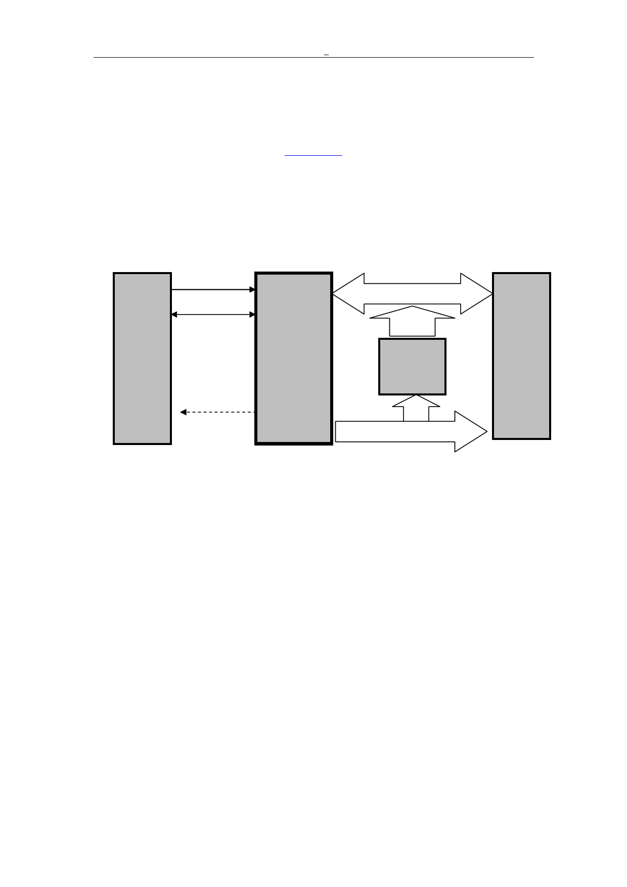
1. Introduction
CH455 is LED display drive and keyboard scan control chip. It sets clock surge circuit
internally to drive four bits number LED or thirty two LEDs dynamically. And at the same time it
can scan 28-key. CH455 exchanges data with MCU via two wires serial interface of SCL and
SDA..
MCU
etc
SCL
SDA
INT#
CH455
(broken line
is optional)
SEG7~SEG0
SEG6 ~
7×4 matrix
28 keys
board
DIG3~DIG0
4 bits
LED
Or
32
LEDs
2. Features
● Set display current drive layer internally, the current of segment is no less than 25mA, the
current of word is no less than 160mA.
● Display scan control dynamically, support 8×4 or 7×4, directly drive four bits number LED or
thirty two LEDs.
● Internal limit current, set eight level light control via space percentage.
● Set 28-key keyboard control, based on 7×4 matrix scan..
● Set pull-down resistor internal while key-press, glitter removable.
● Supply keyboard interrupt active with low-level, and supply key-press release token to check
the key is pressed or release.
● High speed two wires serial interface, the speed of clock varies from 0 to 4MHz, compatible
with I2C bus, save pins.
● Set turn on power to reset, 2.7V~5V power.
● Support low exhaust sleep mode to save energy, awoke via press key or command.
● Set clock surge circuit internally, the external clock or surge equipment is not necessary, resister
to be disturbed.
● Supply DIP18, SOP18 and SOP16 package without lead, compatible with RoHS, the function
and pins are part compatible with CH450 .
1 page 
English DataSheet of CH455
5
SEG6
37H 36H 35H 34H
SEG0+SEG1 3FH 3EH 3DH 3CH
5.4. Serial interface
CH455 has 2-wire serial interface achieved by hardware, contains two main signal wires:
serial data clock input wire SCL, serial data input and output wire SDA; and one assistant signal
wire: interrupt output wire INT#. The SCL is input wire with pull-up resistor, high-level in default;
SDA is bidirectional signal wire with pull-up resistor, high-level in default; INT# is drain open
output with pull-up resistor, after starting keyboard scan function, it is keyboard interrupt output,
high-level in default.
SDA used to input and output serial data, high-level means bit data is 1, low-level means bit
data is 0, the serial data input sequence is high bit in front, and the low bit is behind.
SCL used to supply serial clock. CH455 input data from SDA when SCL is raising, output
data from SDA when SCL is falling.
During SCL is high-level, the SDA is falling, defined as start signal of serial interface.
During SCL is high-level, the SDA is raising, defined as stop signal of serial interface. After
CH455 has checked start signal, it can receive and analyse command. In order to save I/O pin,
keep SDA state, share the SCL with other interface circuit; if make sure the SDA change only
when SCL is low-level, SCL and SDA can share with other interface circuit.
INT# used as keyboard interrupt output, high-level in default. When CH455 has checked the
efficient key-press, INT# output interrupt active with low-level; after MCU is interrupted, execute
read operation to CH455, CH455 will change INT# to high-level, and output key-press code from
SDA, MCU gets one byte data from SDA, key-press code.
The communication process has six steps: output start signal, output byte 1, acknowledge 1,
input byte 2, acknowledge 2, output stop signal. The start signal and the stop signal are as before,
acknowledge 1 and 2 are always 1, the output byte 1and input byte 2 each contains 8-bit data bits,
one byte data.
The following is a write operation, byte 1 is 01001000B, 48H; byte 2 is 00000001B, 01H.
6. Operation command
The operation command of CH455 is divided as three groups. The start command, stop
command, acknowledge 1 and acknowledge 2 are the same, the difference are the output byte 1,
byte 2, the transfer direction of byte 2.
6.1. Set system parameter command
The output byte is 01001000B, 48H; the output byte 2 is 0[INTENS][7SEG][SLEEP]0[ENA]B.
The set system parameter command is used to set CH455 system layer parameters: display and
keyboard scan enable ENA, sleep enable SLEEP, 7-segment mode 7SEG, display light control
INTENS. The command has no influence on the data in internal data buffer.
When ENA is 1, allow display output and keyboard scan; when ENA is 0, close display drive and
5 Page 
English DataSheet of CH455
11
8.5. Anti-jamming (important)
Because current of CH455 drives number LED or LED is large, burr voltage will generated
in power. If power wire or ground wire doesn’t lay logically, it will influence stability of MCU or
CH455. The resolve methods of power jamming are as following:
①, Recommending to use the short and thick power wire and ground wire, especially when
CH455 and MCU are belongs to two PCBs;
②, Near to CH455, and between positive and negative power to parallel connection power
decoupling capacitance, One 0.1uF monolithic or china capacitance and no less than 100uF
electrolytic capacitance are at least.
For the long signal wire, consult the following image:
①, Add capacitance C11 and C12, near to CH455 of signal wire, the capacitance is from
47pF to 470pF. The capacitance is more large, the transfer speed of MCU communication is more
slower;
②, Add R18 and R19 are optional, the value is from 100Ω to 470Ω;
③, Depress the transfer speed between MCU and CH455 (because of adding the capacitance
and resister);
④, Drive by standard I/O pin (such as standard MCS51 MCU), recommend to add R8 and
R9, the value is from 500Ω to 10KΩ, to enhance the pull-up ability of MCS-51 I/O pins, in that
case to keep the better digital signal wave; when the signal wire is short, the R8 and R9 is no need.
For I/O pins with totem pole drive, the R8 and R9 are no need.
Addition, In the strong disturb environment, MCU can refurbish CH455 several seconds
termly. Containing newly load data register of each number LED and newly start displaying.
11 Page | ||
| Páginas | Total 12 Páginas | |
| PDF Descargar | [ Datasheet CH455.PDF ] | |
Hoja de datos destacado
| Número de pieza | Descripción | Fabricantes |
| CH450 | LED drive and keyboard control chip | ETC |
| CH450FPT | SCHOTTKY BARRIER DIODE | Chenmko Enterprise |
| CH452 | Digital tube driver and keyboard control chip | ETC |
| CH455 | LED drive and keyboard control chip | ETC |
| Número de pieza | Descripción | Fabricantes |
| SLA6805M | High Voltage 3 phase Motor Driver IC. |
Sanken |
| SDC1742 | 12- and 14-Bit Hybrid Synchro / Resolver-to-Digital Converters. |
Analog Devices |
|
DataSheet.es es una pagina web que funciona como un repositorio de manuales o hoja de datos de muchos de los productos más populares, |
| DataSheet.es | 2020 | Privacy Policy | Contacto | Buscar |