|
|
|
PDF A8600 Data sheet ( Hoja de datos )
| Número de pieza | A8600 | |
| Descripción | Quadruple Output Regulator | |
| Fabricantes | Allegro MicroSystems | |
| Logotipo | ||
Hay una vista previa y un enlace de descarga de A8600 (archivo pdf) en la parte inferior de esta página. Total 30 Páginas | ||
|
No Preview Available !
A8600
Quadruple Output Regulator with Two High-Side Switches,
BU/ACC Voltage Detectors, and Mute Delay
Features and Benefits
• Four independent, high current switching regulators
• Adjustable 1.0 A/±1.5% always-on asynchronous buck
regulator with an integrated 150 mΩ MOSFET (SW1)
▫ Employs PFM to deliver 3.3 V/40 μA while drawing less
than 50 μA from VIN of 12 V
▫ Operates down to at least 3.6 VIN
• Adjustable 1.5 A/±1.5% asynchronous buck regulator with
an integrated 120 mΩ high-side MOSFET (SW2)
• Adjustable 2.0 A/±1.5% asynchronous buck regulator with
an integrated 110 mΩ MOSFET (SW3)
• Adjustable ±1.5% synchronous buck controller with
integrated gate drivers and current sensing (SW4)
• Fixed 425 kHz, interleaved PWM switching frequency
• EN/SYNC input for PWM frequency scaling
• Adjustable soft-start time for each switching regulator
• All switching regulators provide prebias startup with zero
reverse current
• All switching regulators have overvoltage protection
• External compensation for all switching regulators
Continued on the next page…
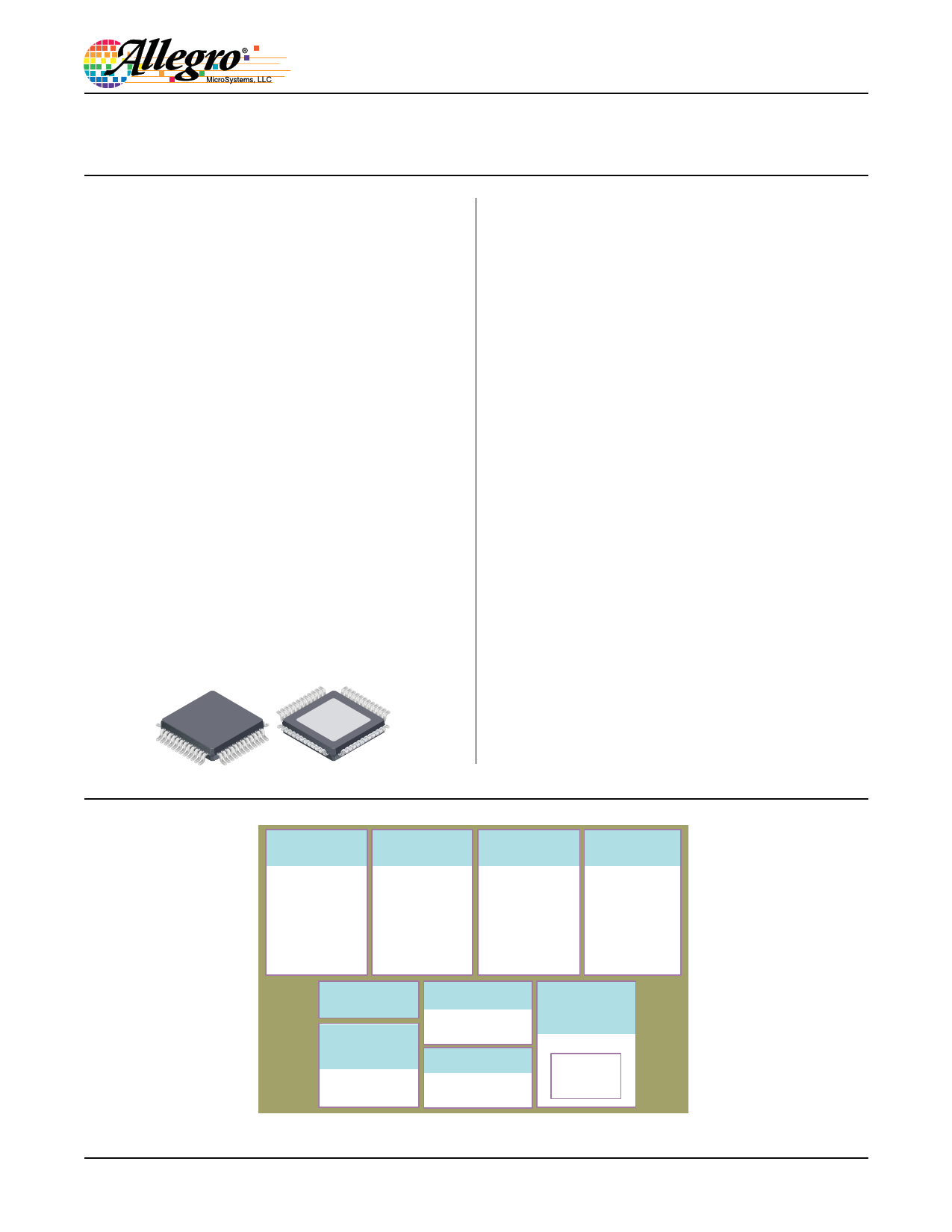
Package: 48-pin LQFP (suffix JP)
Description
Designed to provide the power supply requirements of next
generation car audio and infotainment systems, the A8600
provides all the control and protection circuitry to produce
four high current regulators, each with ±1.5% accuracy. The
A8600 includes control circuitry to implement three adjustable,
asynchronous buck regulators with integrated MOSFETs. Also,
the A8600 provides the control circuitry, gate drivers, and
current sensing to implement a synchronous buck controller
with external MOSFETs. In standby mode, the A8600 draws
less than 50 μA from VIN of 12 V while employing pulse
frequency modulation (PFM) to deliver 3.3 V/40 μA via the
always-on regulator, SW1. The always-on regulator operates
down to at least VIN of 3.6 V (VIN falling).
Features of the A8600 include: an EN/SYNC input to either
turn the A8600 on/off or increase/decrease the base pulse
width modulation (PWM) frequency, four adjustable soft-start
times, and four external compensation pins. Output voltage
monitoring of switchers SW2, SW3, and SW4 is provided
by a single, open-drain POK output. In addition, the A8600
provides two high voltage, high-side switches with foldback
overcurrent protection. These two high-side switches actively
block reverse current. The A8600 also provides direct battery
(BU) and switched (accessory) battery (ACC) detectors and
a mute pulse output with an adjustable delay.
Continued on the next page…
Not to scale
A8600-DS, Rev. 3
Switcher 1
(SW1)
Adjustable
Output Voltage
1.0 AAVG / 2.5 APEAK
Always-On
PWM / PFM
Asynchronous
Buck
Regulator
Switcher 2
(SW2)
Adjustable
Output Voltage
1.5 AAVG / 2.5 APEAK
PWM
Asynchronous
Buck
Regulator
Switcher 3
(SW3)
Adjustable
Output Voltage
2.0 AAVG / 2.5 APEAK
PWM
Asynchronous
Buck
Regulator
Switcher 4
(SW4)
Adjustable
Output Voltage
Adjustable ILIM
PWM
Synchronous
Buck
Controller
Charge
Pump
Enable and
Synchronization
(EN/SYNC)
425 kHz
180° Shift
High-Side Switch 1
(S1)
1.0 Ω Total
with
Foldback Limiting
High-Side Switch 2
(S2)
1.0 Ω Total
with
Foldback Limiting
BU and ACC
Detectors
Mute Pulse
with Delay
Figure 1. A8600 major features
1 page 
A8600
Pin-Out Diagram
Quadruple Output Regulator with Two High-Side Switches,
BU/ACC Voltage Detectors, and Mute Delay
LX2 37
LX2 38
BOOT2 39
SS2 40
FB2 41
COMP2 42
COMP1 43
FB1 44
BIAS 45
SS1 46
BOOT1 47
LX1 48
PAD
24 COMP4
23 POK
22 OUT2
21 VINS
20 OUT1
19 ENS
18 COMP3
17 FB3
16 SS3
15 BOOT3
14 LX3
13 LX3
Name Number
Function
ACCI
8 Input to the ACC comparator
ACCO
7 Output of the ACC comparator
BIAS
45
Bias input, supplies internal circuitry when VSW1
is high enough
BOOT1
47 Floating gate drive for buck regulator SW1
BOOT2
39 Floating gate drive for buck regulator SW2
BOOT3
15 Floating gate drive for buck regulator SW3
BOOT4
31 Floating gate drive for buck regulator SW4
BUI 10 Input to the BU comparator
BUO
COMP1
COMP2
COMP3
9 Output of the BU comparator
43
Error amplifier compensation network for
regulator SW1
42
Error amplifier compensation network for
regulator SW2
18
Error amplifier compensation network for
regulator SW3
COMP4
24
Error amplifier compensation network for
regulator SW4
CSN
26 Current sense pin for buck regulator SW4
CSP
27 Current sense pin for buck regulator SW4
CTMR
5 Delay programming for the Mute pulse circuit
EN/SYNC
6
SWx enable and PFM control, and PWM
synchronization
ENS
19 S1/S2 enable input
FB1 44 Feedback pin for buck regulator SW1
FB2 41 Feedback pin for buck regulator SW2
FB3 17 Feedback pin for buck regulator SW3
Name
FB4
GND
HG4
LG4
LX1
LX2
LX3
LX4
MUTE
NC
OUT1
OUT2
PAD
PGND
POK
SS1
SS2
SS3
SS4
VIN1
VIN2
VIN3
VINS
VREG
Number
Function
25 Feedback pin for buck regulator SW4
3 Ground
29 High side gate drive for buck regulator SW4
32 Low side gate drive for buck regulator SW4
48 Switching node for buck regulator SW1
37, 38 Switching node for buck regulator SW2
13, 14 Switching node for buck regulator SW3
30 Switching node for buck regulator SW4
2
Open-drain, active low output of the Mute pulse
circuit
34 Unused
20 High-side switch S1 output
22 High-side switch S2 output
– Exposed pad for enhanced thermal dissipation
33 Power ground
23 Power OK open drain output
46 Soft start programming for regulator SW1
40 Soft start programming for regulator SW2
16 Soft start programming for regulator SW3
28 Soft start programming for regulator SW4
1 Input supply for buck regulator SW1
35, 36 Input supply for buck regulator SW2
11, 12 Input supply for buck regulator SW3 (and SW4)
21 S1/S2 high-side switch input
4 Internal voltage regulator bypass capacitor pin
Allegro MicroSystems, LLC
115 Northeast Cutoff
Worcester, Massachusetts 01615-0036 U.S.A.
1.508.853.5000; www.allegromicro.com
5
5 Page 
A8600
Quadruple Output Regulator with Two High-Side Switches,
BU/ACC Voltage Detectors, and Mute Delay
ELECTRICAL CHARACTERISTICS (continued) Valid at 5.5 V ≤ VINx ≤ 26 V, –40°C ≤ TA ≤ 125ºC, –40°C ≤ TJ ≤ 125ºC;
unless otherwise specified
Characteristic
Symbol
Test Conditions
Min.
Typ.
Max.
SW1 (ALWAYS-ON, LOW IQ, PWM/PFM REGULATOR) (continued)
Error Amplifier (continued)
Output Current
Maximum Output Voltage
Minimum Output Voltage
COMP1 Pull Down Resistance
Pulse Width Modulation (PWM)
IEA1
VEAO(max)1
VEAO(min)1
RCOMP1
VCOMP1 = 1.2 V
Fault condition
− ±75 −
1.3 1.7 2.1
− − 200
−1−
PWM Ramp Offset
Minimum Controllable On-Time
Minimum Switch Off-Time
COMP1 to SW1 Current Gain
Slope Compensation
Overcurrent Protection (OCP)
VPWMOFFSET1 VCOMP1 set for 0% duty cycle
tON(MIN)1
tOFF(MIN)1
gmPOWER1
SE1
− 400 −
80 140 180
40 95 135
− 3.6 −
300 450 600
Pulse-by-Pulse Current Limit
Overvoltage Protection (OVP)
ILIM1
tON1 = tON(MIN)1 , fSW = fOSC
tON1 = (1 / fOSC) – tOFF(MIN)1 , fSW = fOSC
3.9 4.4 4.9
3.0 3.5 4.0
Output Overvoltage Threshold (SW1
Disable)
VOVO1 VFB1 rising, PWM mode
840 860 880
Overvoltage Hysteresis
Soft Start
VOVOHYS1 VFB1 falling, relative to VOVO1
− −10 −
SS1 Hiccup Reset Voltage
VSSRST1
SS1 Switching Frequency
fSS1
SS1 Startup (Source) Current1
ISSSU1
SS1 Hiccup (Sink) Current1
ISSHIC1
SS1 Delay Time
tdSS1
SS1 Ramp Time
tSSRAMP1
SS1 Pull Down Resistance
RSSFLT1
Hiccup Mode (PWM only, not in PFM)
VSS1 falling due to RSSFLT1
0 V < VFB1 < 300 mV, VCOMP1 at maximum
0 V < VFB1 < 300 mV
300 mV < VFB1
Hiccup mode disabled (no fault condition)
Hiccup mode enabled
CSS1 = 0.68 μF
CSS1 = 0.68 μF
Fault condition
140
−
−
−
−2.50
0.75
−
−
−
200
fSW1/4
fSW1/2
fSW1
−2.00
1.00
136
272
5
275
−
−
−
−1.50
1.25
−
−
−
Hiccup OCP Enable Threshold
VHICEN1 VSS1 rising
− 2.3 −
Hiccup Operation OCP Count
tOCPLIM1
VSS1 > 2.3 V, VFB1 < 0.3 V
VSS1 > 2.3 V, VFB1 > 0.3 V
− 30 −
− 118 −
Hiccup Operation BOOT Shorted
Count
tBOOTUV1
− 30 −
Hiccup Operation BOOT Open Count tBOOTOPEN1
−7−
Unit
μA
V
mV
kΩ
mV
ns
ns
A/V
mA/μs
A
A
mV
mV
mV
kHz
kHz
kHz
μA
μA
ms
ms
kΩ
V
PWM
cycles
PWM
cycles
PWM
cycles
PWM
cycles
Continued on the next page…
Allegro MicroSystems, LLC
115 Northeast Cutoff
Worcester, Massachusetts 01615-0036 U.S.A.
1.508.853.5000; www.allegromicro.com
11
11 Page | ||
| Páginas | Total 30 Páginas | |
| PDF Descargar | [ Datasheet A8600.PDF ] | |
Hoja de datos destacado
| Número de pieza | Descripción | Fabricantes |
| A8600 | Quadruple Output Regulator | Allegro MicroSystems |
| A8600 | WHITE LED BACKLIGHT DRIVER SIX-STRING | AiT Semiconductor |
| A8600EJPTR-T | Quadruple Output Regulator | Allegro MicroSystems |
| A8601 | Multiple-Output Regulator | Allegro |
| Número de pieza | Descripción | Fabricantes |
| SLA6805M | High Voltage 3 phase Motor Driver IC. |
Sanken |
| SDC1742 | 12- and 14-Bit Hybrid Synchro / Resolver-to-Digital Converters. |
Analog Devices |
|
DataSheet.es es una pagina web que funciona como un repositorio de manuales o hoja de datos de muchos de los productos más populares, |
| DataSheet.es | 2020 | Privacy Policy | Contacto | Buscar |