|
|
|
PDF APL5930 Data sheet ( Hoja de datos )
| Número de pieza | APL5930 | |
| Descripción | Ultra Low Dropout (0.23V Typical) Linear Regulator | |
| Fabricantes | ANPEC | |
| Logotipo | ||
Hay una vista previa y un enlace de descarga de APL5930 (archivo pdf) en la parte inferior de esta página. Total 17 Páginas | ||
|
No Preview Available !
APL5930
3A, Ultra Low Dropout (0.23V Typical) Linear Regulator
Features
General Description
• Compatible with APL5913
The APL5930 is a 3A ultra low dropout linear regulator.
• Ultra Low Dropout
The IC needs two supply voltages, one is a control voltage
- 0.23V(typical) at 3A Output Current
• Low ESR Output Capacitor (Multi-layer
Chip Capacitors (MLCC)) Applicable
• 0.8V Reference Voltage
• High Output Accuracy
(V ) for the control circuitry, the other is a main supply
CNTL
voltage (VIN) for power conversion, to reduce power dissi-
pation and provide extremely low dropout voltage.
The APL5930 integrates many functions. A Power-On-
Reset (POR) circuit monitors both supply voltages on
VCNTL and VIN pins to prevent erroneous operations.
- ±1.5% over Line, Load, and Temperature Range The functions of thermal shutdown and current-limit pro-
• Fast Transient Response
tect the device against thermal and current over-loads. A
• Adjustable Output Voltage
POK indicates the output voltage status with a delay time
• Power-On-Reset Monitoring on Both VCNTL and set internally. It can control other converter for power
VIN Pins
sequence. The APL5930 can be enabled by other power
• Internal Soft-Start
systems. Pulling and holding the EN voltage below 0.4V
• Current-Limit and Short Current-Limit Protections shuts off the output.
The APL5930 is available in a SOP-8P package which
• Thermal Shutdown with Hysteresis
features small size as SOP-8 and an Exposed Pad to
• Open-Drain VOUT Voltage Indicator (POK)
reduce the junction-to-case resistance to extend power
• Low Shutdown Quiescent Current (<30 µA)
range of applications.
• Shutdown/Enable Control Function
• Simple SOP-8P Package with Exposed Pad
Applications
• Lead Free and Green Devices Available
• Front Side Bus VTT (1.2V/3A)
(RoHS Compliant)
• Note Book PC Applications
• Motherboard Applications
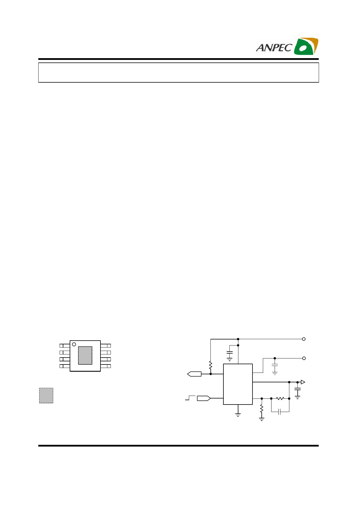
Pin Configuration
Simplified Application Circuit
GND 1
FB 2
VOUT 3
VOUT 4
8 EN
7 POK
6 VCNTL
5 VIN
SOP-8P (Top View)
= Exposed Pad
(connected to VIN plane for better heat dissipation)
POK
EN
Enable
VCNTL
POK VIN
VOUT
APL5930
EN FB
GND
VCNTL
VIN
VOUT
Optional
ANPEC reserves the right to make changes to improve reliability or manufacturability without notice, and
advise customers to obtain the latest version of relevant information to verify before placing orders.
Copyright © ANPEC Electronics Corp.
Rev. A.4 - Sep., 2009
1
www.anpec.com.tw
1 page 
APL5930
Typical Operating Characteristics
Current-Limit vs. Junction
Temperature
6.5
VOUT = 1.2V
6.0 VCNTL = 5V
5.5
5.0
VCNTL = 3.3V
4.5
4.0
3.5
-50
-25
0
25 50 75 100 125
Junction Temperature (oC)
Dropout Voltage vs. Output Current
450
400
VCNTL = 5V
VOUT = 1.2V
350
300
250
200
TJ = 125 C
TJ = 75 C
TJ = 25 C
150
100
TJ = 0 C
50 TJ = - C
0
0 0.5 1 1.5 2 2.5 3
Output Current, IOUT (A)
Dropout Voltage vs. Output Current
400
VCNTL = 5V
350 VOUT = 1.5V
300
250
200
TJ = 125 C
TJ = 75 C
TJ = 25 C
150
100
50
0
0
TJ = -
TJ = 0 C
C
0.5 1 1.5 2 2.5
Output Current, IOUT (A)
3
Copyright © ANPEC Electronics Corp.
Rev. A.4 - Sep., 2009
5
Short Current-Limit vs. Junction
Temperature
1.20
1.18
1.16
1.14
1.12
VCNTL = 5V
1.10
1.08
1.06
1.04
VCNTL = 3.3V
1.02
1.00
Junction Temperature (oC)
Droput Voltage vs. Output Current
450
400
VCNTL = 3.3V
VOUT = 1.2V
350
300
250
TJ = 125 C
TJ = 75 C
TJ = 25 C
200
150
100
TJ = 0 C
50 TJ = - C
0
0 0.5 1 1.5 2 2.5 3
Output Current, IOUT (A)
Dropout Voltage vs. Output Current
400
350
VCNTL = 5V
VOUT = 1.8V
300
250
200
TJ = 125 C
TJ = 75 C
TJ = 25 C
150
100 TJ = 0 C
50 TJ = - C
0
0 0.5 1 1.5 2 2.5 3
Output Current, IOUT (A)
www.anpec.com.tw
5 Page 
APL5930
Application Information
Power Sequencing
The power sequencing of VIN and VCNTL is not neces-
sary to be concerned. However, do not apply a voltage to
VOUT for a long time when the main voltage applied at
VIN is not present. The reason is the internal parasitic
diode from VOUT to VIN conducts and dissipates power
without protections due to the forward-voltage.
Output Capacitor
The APL5930 requires a proper output capacitor to main-
tain stability and improve transient response. The output
capacitor selection is dependent upon ESR (equivalent
series resistance) and capacitance of the output capaci-
tor over the operating temperature.
Ultra-low-ESR capacitors (such as ceramic chip
capacitors) and low-ESR bulk capacitors (such as solid
tantalum, POSCap, and Aluminum electrolytic capacitors)
can all be used as output capacitors.
During load transients, the output capacitors, depending
on the stepping amplitude and slew rate of load current,
are used to reduce the slew rate of the current seen by
the APL5930 and help the device to minimize the varia-
tions of output voltage for good transient response. For
the applications with large stepping load current, the low-
ESR bulk capacitors are normally recommended.
Decoupling ceramic capacitors must be placed at the
load and ground pins as close as possible and the im-
pedance of the layout must be minimized.
Ultra-low-ESR capacitors (such as ceramic chip capaci-
tors) and low-ESR bulk capacitors (such as solid
tantalum, POSCap, and Aluminum electrolytic capacitors)
can all be used as an input capacitor of VIN. For most
applications, the recommended input capacitance of VIN
is 10µF at least. However, if the drop of the input voltage
is not cared, the input capacitance can be less than 10µF.
More capacitance reduces the variations of the supply
voltage on VIN pin.
Setting Output Voltage
The output voltage is programmed by the resistor divider
connected to FB pin. The preset output voltage is calcu-
lated by the following equation :
VOUT
=
0.8
⋅
1 +
R1
R2
........... (V)
Where R1 is the resistor connected from VOUT to FB with
Kelvin sensing connection and R2 is the resistor con-
nected from FB to GND. A bypass capacitor(C1) may be
connected with R1 in parallel to improve load transient
response and stability.
Input Capacitor
The APL5930 requires proper input capacitors to supply
current surge during stepping load transients to prevent
the input voltage rail from dropping. Because the para-
sitic inductor from the voltage sources or other bulk ca-
pacitors to the VIN pin limit the slew rate of the surge
currents, more parasitic inductance needs more input
capacitance.
Copyright © ANPEC Electronics Corp.
Rev. A.4 - Sep., 2009
11
www.anpec.com.tw
11 Page | ||
| Páginas | Total 17 Páginas | |
| PDF Descargar | [ Datasheet APL5930.PDF ] | |
Hoja de datos destacado
| Número de pieza | Descripción | Fabricantes |
| APL5930 | Ultra Low Dropout (0.23V Typical) Linear Regulator | ANPEC |
| APL5932A | Ultra Low Dropout (0.3V Typical) Linear Regulator | ANPEC |
| APL5932B | Ultra Low Dropout (0.3V Typical) Linear Regulator | ANPEC |
| APL5932C | Ultra Low Dropout (0.3V Typical) Linear Regulator | ANPEC |
| Número de pieza | Descripción | Fabricantes |
| SLA6805M | High Voltage 3 phase Motor Driver IC. |
Sanken |
| SDC1742 | 12- and 14-Bit Hybrid Synchro / Resolver-to-Digital Converters. |
Analog Devices |
|
DataSheet.es es una pagina web que funciona como un repositorio de manuales o hoja de datos de muchos de los productos más populares, |
| DataSheet.es | 2020 | Privacy Policy | Contacto | Buscar |