|
|
|
PDF LTC6950 Data sheet ( Hoja de datos )
| Número de pieza | LTC6950 | |
| Descripción | 1.4GHz Low Phase Noise / Low Jitter PLL | |
| Fabricantes | Linear Technology | |
| Logotipo | ||
Hay una vista previa y un enlace de descarga de LTC6950 (archivo pdf) en la parte inferior de esta página. Total 30 Páginas | ||
|
No Preview Available !
Features
LTC6950
1.4GHz Low Phase Noise,
Low Jitter PLL with Clock
Distribution
Description
n Low Phase Noise and Jitter
n Additive Jitter: 18fsRMS (12kHz to 20MHz)
n Additive Jitter: 85fsRMS (10Hz to Nyquist)
n EZSync™ Multichip Clock Edge Synchronization
n Full PLL Core with Lock Indicator
n –226dBc/Hz Normalized In-Band Phase Noise Floor
n –274dBc/Hz Normalized 1/f Phase Noise
n 1.4GHz Maximum VCO Input Frequency
n Four Independent, Low Noise 1.4GHz LVPECL Outputs
n One LVDS/CMOS Configurable Output
n Five Independently Programmable Dividers Covering
All Integers from 1 to 63
n Five Independently Programmable VCO Clock Cycle
Delays Covering All Integers from 0 to 63
n –40°C to 105°C Junction Temperature Range
Applications
n Clocking High Speed, High Resolution ADCs,
DACs and Data Acquisition Systems
n Low Jitter Clock Generation and Distribution
The LTC®6950 is a low phase noise integer-N frequency
synthesizer core with clock distribution. The LTC6950
delivers the low phase noise clock signals demanded in
high frequency, high resolution data acquisition systems.
The frequency synthesizer contains afull low noise PLL core
with a programmable reference divider (R), a programmable
feedback divider (N), a phase/frequency detector (PFD)
and a low noise charge pump (CP). The clock distribution
section of the LTC6950 delivers up to five outputs based on
the VCO input. Each output is individually programmed to
divide the VCO input frequency by any integer from 1 to 63
and to delay the output by 0 to 63 VCO clock cycles. Four
of the outputs feature very low noise, low skew LVPECL
logic signals capable of operation up to 1.4GHz. The fifth
output is selectable as either an LVDS (800MHz) or CMOS
(250MHz) logic type. This output is also programmed to
produce an output signal based on either the VCO input
or the reference divider output.
L, LT, LTC, LTM, Linear Technology and the Linear logo are registered trademarks and EZSync
and ClockWizard are trademarks of Linear Technology Corporation. All other trademarks are
the property of their respective owners. Protected by U.S. Patents, including 8,319,551 and
8,819,472.
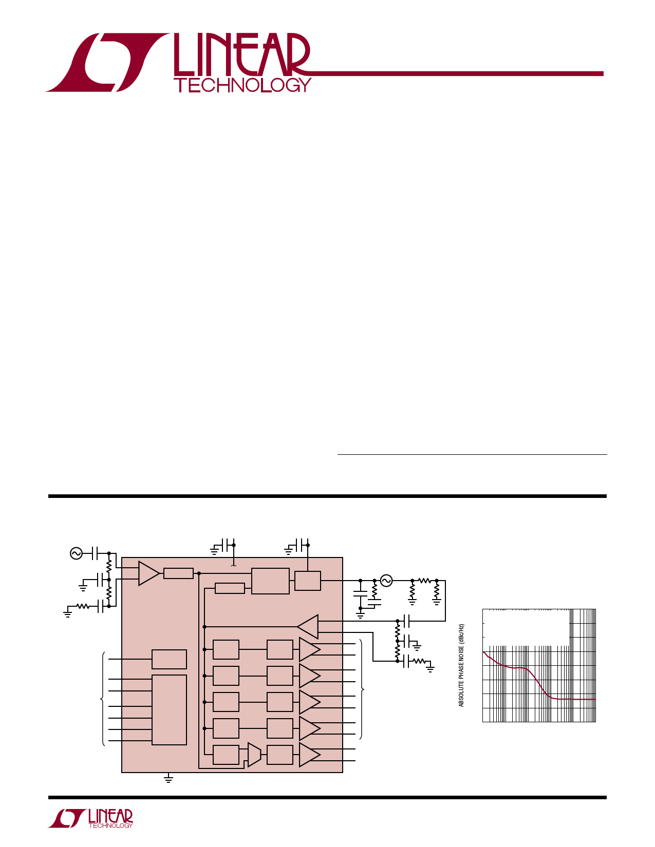
Typical Application
100MHz
REF
OSC
0.1µF
49.9Ω
0.1µF
REF+
REF–
R DIVIDER
3.3V
1µF
V+
49.9Ω
N DIVIDER
49.9Ω 0.1µF
TO/FROM
PROCESSOR
SYNC
STAT2
STAT1
SDO
SDI
SCLK
CS
SYNC
CONTROL
SERIAL
PORT
GND
DELAY
0 TO 63
DELAY
0 TO 63
DELAY
0 TO 63
DELAY
0 TO 63
DELAY
0 TO 63
5V
1µF
PHASE
FREQUENCY
DETECTOR
VCP+
LTC6950
CHARGE
PUMP
CP
8.2nF
1GHz VCSO
CRYSTEK
CVCSO-914-1000
422Ω 150Ω
37.4Ω
150Ω
DIVIDE
1 TO 63
DIVIDE
1 TO 63
DIVIDE
1 TO 63
DIVIDE
1 TO 63
DIVIDE
1 TO 63
VCO+
VCO–
PECL0+
PECL0–
PECL1+
PECL1–
PECL2+
PECL2–
PECL3+
PECL3–
LV/CM+
LV/CM–
0.1µF 0.01µF
49.9Ω
49.9Ω
0.01µF
49.9Ω
TO
ADC OR
DAC
0.01µF
TO FPGA
6950 TA01a
For more information www.linear.com/LTC6950
PECLx Closed-Loop Phase Noise,
fVCSOf=PE1CGLxH=z,1M25xM[5H:0z] = 8,
–100
–110
–120
NOTES 8, 11, 15
RMS JITTER = 93fs
(INTEGRATED 100Hz TO 62.5MHz)
fPFD = 100MHz
LOOP BW = 12kHz
–130
–140
–150
–160
–170
–180
100
1k 10k 100k 1M 10M
OFFSET FREQUENCY (Hz)
6950 TA01b
6950f
1
1 page 
LTC6950
E lectrical Characteristics The l denotes the specifications which apply over the full operating
jVuCnPc+ti=on5Vteumnpleesrsatoutrheerrawnigsee,soptehceirfiweids.eAslpl evcoilftiacgaetisonasreawreitahtrTeAsp=e2c5t °toC
(Note 2).
ground.
V+
=
VREF+
=
VVCO+
=
VP0+
=
VP1+
=
VP2+
=
VP3+
=
3.3V,
SYMBOL PARAMETER
CONDITIONS
MIN TYP MAX UNITS
Output Divider (M)
Mx[5:0]
Divider Range
M0[5:0], M1[5:0], M2[5:0], M3[5:0],
M4[5:0]
All Integers Included
l1
63 Cycles
DELx[5:0] Divider Delay in VCO Clock Cycles
DEL0[5:0], DEL1[5:0], DEL2[5:0],
DEL3[5:0], DEL4[5:0]
All Integers Included
l0
63 Cycles
PECLx Clock Outputs (PECL0+, PECL0–, PECL1+, PECL1–, PECL2+, PECL2–, PECL3+, PECL3–)
fPECLx
VCM
|VOD|
tRISE
Frequency
Common Mode Voltage (Outputs Static)
Differential Voltage (Outputs Static)
Rise Time, 20% to 80%
Single-Ended Termination = 50Ω to (VPx+ – 2V) l
1400
Single-Ended Termination = 50Ω to (VPx+ – 2V) l VPx+ – 1.68 VPx+ – 1.48 VPx+ – 1.25
Single-Ended Termination = 50Ω to (VPx+ – 2V) l
Differential Termination = 100Ω, Internal Bias On
610
800 1050
800
Single-Ended Termination
Differential Termination =
1=0500ΩΩ, Itnote(rVnPaxl+B–ia2sVO)n
135
135
MHz
V
mVPK
mVPK
ps
ps
tFALL Fall Time, 80% to 20%
Single-Ended Termination
Differential Termination =
1=0500ΩΩ, Itnote(rVnPaxl+B–ia2sVO)n
135
135
ps
ps
DCPECL
Duty Cycle
Mx[5:0] = 1
Mx[5:0] > 1 (Even or Odd)
l 45
DC5V0CO
55
%
%
tPDP3
Propagation Delay from VCO to PECL3
M3[5:0] = 1, FILTV = 0
M3[5:0] = 1, FILTV = 1
M3[5:0] > 1, FILTV = 0
l 285 495 660
700
l 335 560 745
ps
ps
ps
Propagation Delay from VCO to PECL3,
Temperature Variation
M3[5:0] = 1, FILTV = 0
M3[5:0] = 1, FILTV = 1
M3[5:0] > 1, FILTV = 0
l 0.35
l 0.50
l 0.45
ps/°C
ps/°C
ps/°C
tSKEWPx Skew, from PECL3 to PECL0
M0[5:0] = M3[5:0] = 1
M0[5:0] = M3[5:0] > 1
l –50
l –50
–1.0
–1.5
50
50
ps
ps
Skew, from PECL3 to PECL1
M1[5:0] = M3[5:0] = 1
M1[5:0] = 1, M3[5:0] > 1
M1[5:0] > 1, M3[5:0] = 1
M1[5:0] = M3[5:0] > 1
l –50
l –125
l5
l –50
4.5
–60
69
5
50
0
135
50
ps
ps
ps
ps
Skew, from PECL3 to PECL2
M2[5:0] = M3[5:0] = 1
M2[5:0] = M3[5:0] > 1
l –50
l –50
5
5.5
50
50
ps
ps
Skew, All PECLx Outputs
FILTV = 0, Same Part
l
55 ps
Skew, Same PECLx Output
FILTV = 0, Across Multiple Parts (Note 4)
l
320 ps
Skew, All PECLx Outputs
FILTV = 0, Across Multiple Parts (Note 5)
l
330 ps
For more information www.linear.com/LTC6950
6950f
5
5 Page 
LTC6950
E lectrical Characteristics The l denotes the specifications which apply over the full operating
jVuCnPc+ti=on5Vteumnpleesrsatoutrheerrawnigsee,soptehceirfiweids.eAslpl evcoilftiacgaetisonasreawreitahtrTeAsp=e2c5t °toC
(Note 2).
ground.
V+
=
VREF+
=
VVCO+
=
VP0+
=
VP1+
=
VP2+
=
VP3+
=
3.3V,
SYMBOL PARAMETER
CONDITIONS
MIN TYP MAX UNITS
Phase Noise: Distribution Only
fVCO = 622.08MHz, M4[5:0] = 4,
fLVDS = 155.52MHz
10Hz Offset
100Hz Offset
1kHz Offset
10kHz Offset
100kHz Offset
>1MHz Offset
–125 dBc/Hz
–134 dBc/Hz
–147 dBc/Hz
–154 dBc/Hz
–158 dBc/Hz
–159 dBc/Hz
Jitter: Distribution Only
ffVLVCDOS==612525.0.582MMHHzz, M4[5:0] = 4,
Phase Noise: Distribution Only
fVCO = 622.08MHz, M4[5:0] = 16,
fLVDS = 38.88MHz
12kHz to 20MHz Integration Bandwidth
10Hz to 77.76MHz Integration Bandwidth
10Hz Offset
100Hz Offset
1kHz Offset
10kHz Offset
100kHz Offset
>1MHz Offset
73
138
ffssRRMMSS
–137 dBc/Hz
–145 dBc/Hz
–156 dBc/Hz
–164 dBc/Hz
–165 dBc/Hz
–165 dBc/Hz
VCO to CMOS Additive Phase Noise/Time Jitter (Note 7)
Phase Noise: Distribution Only
fVCO = 245.76MHz, M4[5:0] = 1,
fCMOS = 245.76MHz
10Hz Offset
100Hz Offset
1kHz Offset
10kHz Offset
100kHz Offset
>1MHz Offset
–120
–130
–143
–150.5
–155
–157
dBc/Hz
dBc/Hz
dBc/Hz
dBc/Hz
dBc/Hz
dBc/Hz
Jitter: Distribution Only
ffVCCMOOS=
245.76MHz, M4[5:0]
= 245.76MHz
=
1,
Phase Noise: Distribution Only
fVCO = 245.76MHz, M4[5:0] = 4,
fCMOS = 61.44MHz
12kHz to 20MHz integration bandwidth
10Hz to 122.88MHz integration bandwidth
10Hz Offset
100Hz Offset
1kHz Offset
10kHz Offset
100kHz Offset
>1MHz Offset
57
135
ffssRRMMSS
–132 dBc/Hz
–140 dBc/Hz
–153 dBc/Hz
–161 dBc/Hz
–164 dBc/Hz
–164 dBc/Hz
Jitter: Distribution Only
fVCO = 245.76MHz, M4[5:0] = 4,
fCMOS = 61.44MHz
Phase Noise: Distribution Only
fVCO = 622.08MHz, M4[5:0] = 4,
fCMOS = 155.52MHz
12kHz to 20MHz Integration Bandwidth
10Hz to 30.72MHz integration bandwidth
10Hz Offset
100Hz Offset
1kHz Offset
10kHz Offset
100kHz Offset
>1MHz Offset
104
125
ffssRRMMSS
–125 dBc/Hz
–135 dBc/Hz
–146 dBc/Hz
–155 dBc/Hz
–159 dBc/Hz
–160 dBc/Hz
Jitter: Distribution Only
fVCO = 622.08MHz, M4[5:0] = 4,
fCMOS = 155.52MHz
Phase Noise: Distribution Only
fVCO = 622.08MHz, M4[5:0] = 16,
fCMOS = 38.88MHz
12kHz to 20MHz Integration Bandwidth
10Hz to 77.76MHz Integration Bandwidth
10Hz Offset
100Hz Offset
1kHz Offset
10kHz Offset
100kHz Offset
>1MHz Offset
65 fsRMS
125 fsRMS
–136 dBc/Hz
–146 dBc/Hz
–157 dBc/Hz
–163 dBc/Hz
–165 dBc/Hz
–165 dBc/Hz
For more information www.linear.com/LTC6950
6950f
11
11 Page | ||
| Páginas | Total 30 Páginas | |
| PDF Descargar | [ Datasheet LTC6950.PDF ] | |
Hoja de datos destacado
| Número de pieza | Descripción | Fabricantes |
| LTC695 | Microprocessor Supervisory Circuits | Linear Technology |
| LTC695-3.3 | 3.3V Microprocessor Supervisory Circuits | Linear Technology |
| LTC6950 | 1.4GHz Low Phase Noise / Low Jitter PLL | Linear Technology |
| LTC6957-1 | Dual Output Buffer/Driver/Logic Converter | Linear |
| Número de pieza | Descripción | Fabricantes |
| SLA6805M | High Voltage 3 phase Motor Driver IC. |
Sanken |
| SDC1742 | 12- and 14-Bit Hybrid Synchro / Resolver-to-Digital Converters. |
Analog Devices |
|
DataSheet.es es una pagina web que funciona como un repositorio de manuales o hoja de datos de muchos de los productos más populares, |
| DataSheet.es | 2020 | Privacy Policy | Contacto | Buscar |