|
|
|
PDF Si3050 Data sheet ( Hoja de datos )
| Número de pieza | Si3050 | |
| Descripción | PROGRAMMABLE VOICE DAA SOLUTIONS | |
| Fabricantes | Silicon Laboratories | |
| Logotipo | ||
Hay una vista previa y un enlace de descarga de Si3050 (archivo pdf) en la parte inferior de esta página. Total 30 Páginas | ||
|
No Preview Available !
Si3050+Si3011/18/19
PROGRAMMABLE VOICE DAA SOLUTIONS
Features
PCM highway data interface
µ-law/A-law companding
SPI control interface
GCI interface
80 dB dynamic range TX/RX
Line voltage monitor
Loop current monitor
+6 dBm or +3.2 dBm TX/RX level
mode
Parallel handset detection
3 µA on-hook line monitor current
Overload detection
Programmable line interface
AC termination
DC termination
Ring detect threshold
Ringer impedance
TIP/RING polarity detection
Integrated codec and 2- to 4-wire
analog hybrid
Programmable digital hybrid for
near-end echo reduction
Polarity reversal detection
Programmable digital gain in 0.1 dB
increments
Integrated ring detector
Type I and II caller ID support
Pulse dialing support
3.3 V power supply
Daisy-chaining for up to 16 devices
Greater than 5000 V isolation
Patented isolation technology
Ground start and loop start support
Available in Pb-free RoHS-compliant
packages
Applications
DSL IADs
VoIP gateways
PBX and IP-PBX systems
Voice mail systems
DECT base stations
Description
The Si3050+Si3011/18/19 Voice DAA chipset provides a highly-programmable
and globally-compliant foreign exchange office (FXO) analog interface. The
solution implements Silicon Laboratories' patented isolation capacitor technology,
which eliminates the need for costly isolation transformers, relays, or
opto-isolators, while providing superior surge immunity for robust field
performance. The Voice DAA is available as a chipset, a system-side device
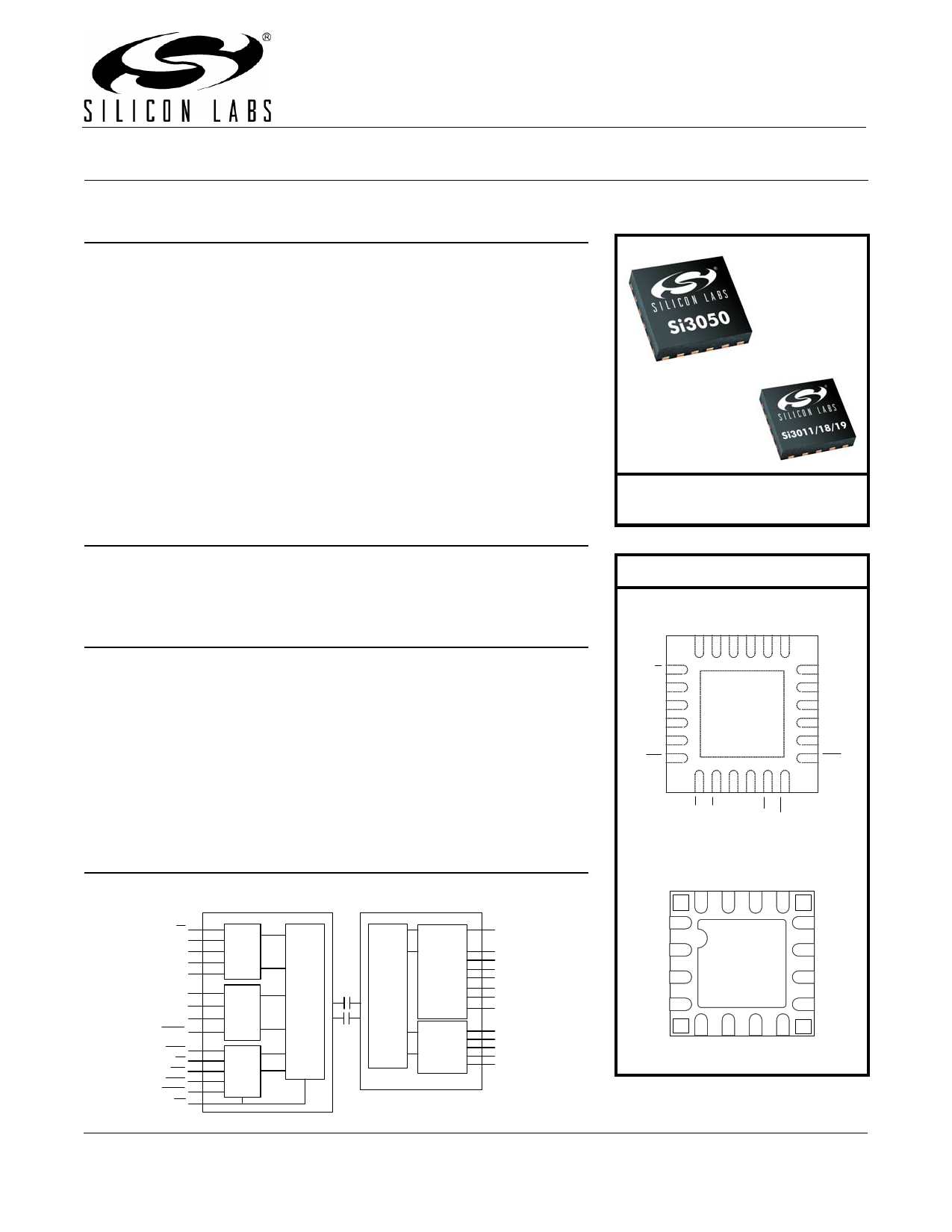
(Si3050) paired with a line-side device (Si3011/18/19). The Si3050 is available in
a 20-pin TSSOP or a 24-pin QFN. The Si3011/18/19 is available in a 16-pin
TSSOP, a 16-pin SOIC, or a 20-pin QFN and requires minimal external
components. The Si3050 interfaces directly to standard telephony PCM
interfaces.
Functional Block Diagram
Ordering Information
See page 106.
Package Options
Si3050
CS 1
FSYNC 2
PCKLK 3
DTX 4
DRX 5
RGDT 6
Si3050
Top View
GND
18 GND
17 VDD
16 VA
15 C1A
14 C2A
13 RESET
Si3011/18/19
CS
SCLK
SDI
SDO
SDI THRU
PCLK
DTX
DRX
FSYNC
RGDT
RG
TGD
TGDE
RESET
AOUT/INT
Si3050
Control
Data
Interface
Line
Data
Interface
Isolation
Interface
Control
Logic
Si3018/19
Isolation
Interface
Hybrid, AC
and DC
Terminations
Ring Detect
Off-Hook
RX
IB
SC
DCT
VREG
VREG2
DCT2
DCT3
RNG1
RNG2
QB
QE
QE2
NC 1 20 19 18 17 16
RX 2
15 DCT3
IB 3
C1B 4
IGND
PAD
14 QB
13 QE2
C2B 5
12 SC
6 7 8 9 10 11 NC
US Patent# 5,870,046
US Patent# 6,061,009
Rev. 1.5 10/11
Copyright © 2011 by Silicon Laboratories
Si3050 + Si3011/18/19
1 page 
Si3050 + Si3011/18/19
1. Electrical Specifications
Table 1. Recommended Operating Conditions and Thermal Information
Parameter1
Symbol
Test Condition
Min2 Typ Max2 Unit
Ambient Temperature
F-Grade
0 25 70
TA °C
G-Grade
–40 25
85
Si3050 Supply Voltage, Digital
Thermal Resistance (Si3011/18/19)3
VD
JA
SOIC-16
TSSOP-16
3.0 3.3 3.6
V
— 77 —
— 89 — °C/W
QFN-20
— 120 —
Thermal Resistance (Si3050)3
JA TSSOP-20 — 84 —
°C/W
QFN-24
— 67 —
Notes:
1. The Si3050 specifications are guaranteed when the typical application circuit (including component tolerance) and any
Si3050 and any Si3011/18/19 are used. See "2. Typical Application Schematic" on page 17 for the typical application
circuit.
2. All minimum and maximum specifications are guaranteed and apply across the recommended operating conditions.
Typical values apply at nominal supply voltages and an operating temperature of 25 °C unless otherwise stated.
3. Operation above 125 °C junction temperature may degrade device reliability.
Rev. 1.5
5
5 Page 
Si3050 + Si3011/18/19
Table 7. Switching Characteristics—Serial Peripheral Interface
(VIO = 3.0 to 3.6 V, TA = 0 to 70 °C, CL = 20 pF)
Parameter*
Cycle Time SCLK
Rise Time, SCLK
Fall Time, SCLK
Delay Time, SCLK Fall to SDO Active
Delay Time, SCLK Fall to SDO
Transition
Delay Time, CS Rise to SDO Tri-state
Setup Time, CS to SCLK Fall
Hold Time, SCLK to CS Rise
Setup Time, SDI to SCLK Rise
Hold Time, SCLK Rise to SDI Transition
Delay time between chip selects
Propagation Delay, SDI to SDITHRU
Symbol
Test
Conditions
tc
tr
tf
td1
td2
Min
61.03
—
—
—
—
td3 —
tsu1 25
th1 20
tsu2 25
th2 20
tcs 220
—
Typ
—
—
—
—
—
—
—
—
—
—
—
6
Max
—
25
25
20
20
20
—
—
—
—
—
—
Unit
ns
ns
ns
ns
ns
ns
ns
ns
ns
ns
ns
ns
*Note: All timing (except Rise and Fall time) is referenced to the 50% level of the waveform. Input test levels are
VIH = VD – 0.4 V, VIL = 0.4 V. Rise and Fall times are referenced to the 20% and 80% levels of the waveform.
SCLK
CS
SDI
SDO
tr
tsu1
td1
tc
tsu2 th2
td2
tf
th1 tcs
td3
Figure 3. SPI Timing Diagram
Rev. 1.5
11
11 Page | ||
| Páginas | Total 30 Páginas | |
| PDF Descargar | [ Datasheet Si3050.PDF ] | |
Hoja de datos destacado
| Número de pieza | Descripción | Fabricantes |
| Si3050 | PROGRAMMABLE VOICE DAA SOLUTIONS | Silicon Laboratories |
| SI3050C | (SI-3100C Series) 5-Terminal / Multi-Function / Full-Mold / Low Dropout Voltage Dropper Type | Allegro Microsystems |
| SI3050N | (SI-3100 Series) 3-Terminal / Full-Mold / Low Dropout Voltage Dropper Type | Allegro Microsystems |
| SI3052V | 3-Terminal/ Low Dropout Voltage Dropper Type | Sanken electric |
| Número de pieza | Descripción | Fabricantes |
| SLA6805M | High Voltage 3 phase Motor Driver IC. |
Sanken |
| SDC1742 | 12- and 14-Bit Hybrid Synchro / Resolver-to-Digital Converters. |
Analog Devices |
|
DataSheet.es es una pagina web que funciona como un repositorio de manuales o hoja de datos de muchos de los productos más populares, |
| DataSheet.es | 2020 | Privacy Policy | Contacto | Buscar |