|
|
PDF GL8088s Data sheet ( Hoja de datos )
| Número de pieza | GL8088s | |
| Descripción | Navigation Receiver Module | |
| Fabricantes | HABNA | |
| Logotipo |  |
|
Hay una vista previa y un enlace de descarga de GL8088s (archivo pdf) en la parte inferior de esta página. Total 18 Páginas | ||
|
No Preview Available !
Navigation Receiver Module
GL8088s
Operations Manual
Version 1.1
Saint Petersburg
2011
1 page 
GL8088s Navigation Receiver
Operations Manual 1.1
General Information
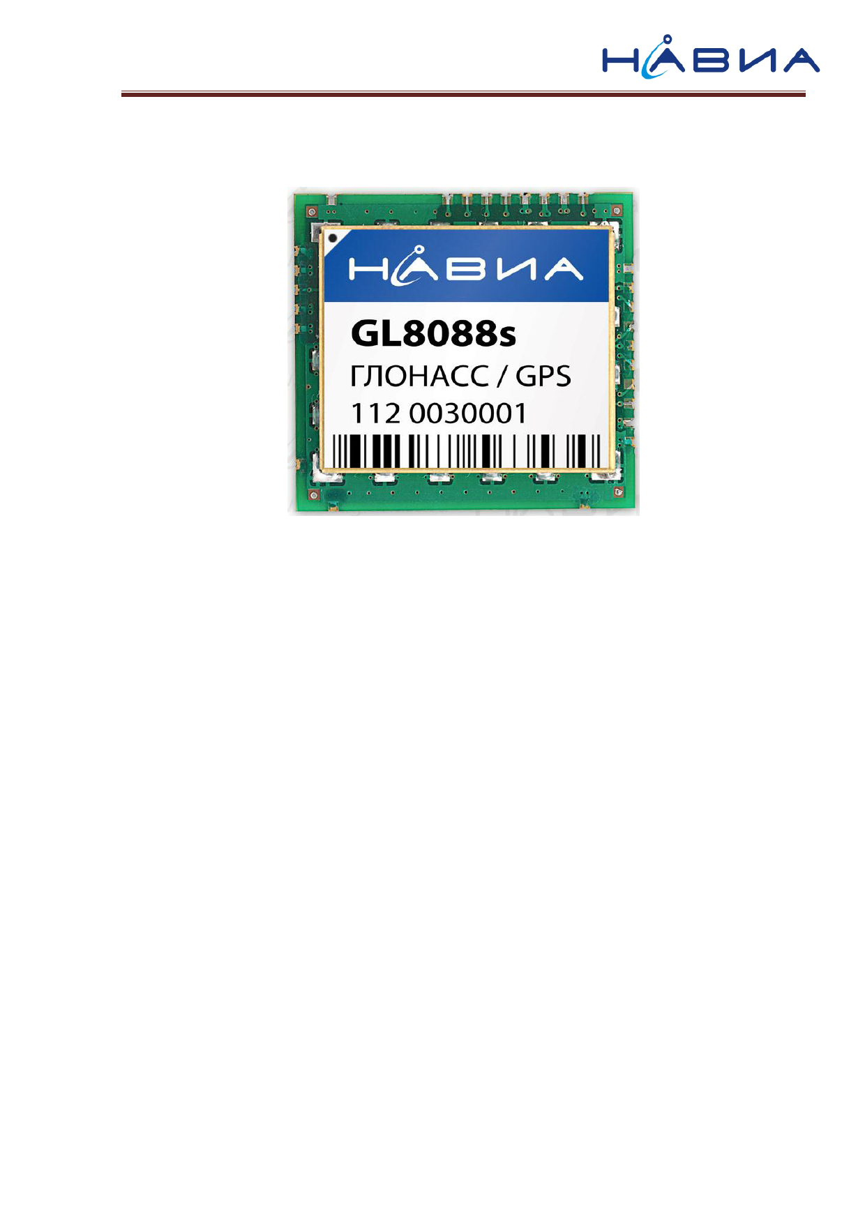
The exterior view of GL8088s navigation receiver module is shown in figure 1.
Fig. 1. The exterior view of the receiver module.
GL8088s receiving device of GLONASS/GPS/GALILEO multy-constellation Navigation
System (hereinafter referred to as receiver or module) is designed for real-time calculation of
current geographic coordinates and velocity of the target, generation of a time sinchronisation
pulse called 1PPS and exchange with peripherals via RS232 serial ports. The operating principle
of the receiver is based on parallel receiving and processing of signals from navigation
GLONASS SC by 32 counting channels in frequency band L1 (CT or PT code), GPS on L1
frequency (C/A code) and GALILEO on E1 frequency. NT solution results are issued in NMEA
messages format.
GL8088s navigation receiver is built on a state-of-the-art dedicated chipset STA8088F from the
family of so-called "systems-on-a-chip" STA8088FG.
The receiver has high sensitivity, low power consumption and short cold/warm/hot start times.
The receiver is provided with two searching (capturing) channels and 32 channels for satellite
signals tracking, which ensures simultaneous searching for satellite signals of GLONASS and
GPS constellations.
The receiver makes it possible to use stellites almanac and ephemeris data stored in the receiver
memory for initial search of satellite signals; this ensures reduction of cold start time and, which
is more important, makes it possible to perform the cold start when the signals from satellites are
weak. The mentioned datas can be prepared by external sources (and transferred to the receiver
via data links), as well as by the receiver itself. In the latter case, no additional information from
the external sources is required.
The right-orientation key (the mark of the first connection terminal) is a black dot against the
white background; the key is located in the top left corner of the label beside NAVIA logo.
5
5 Page 
GL8088s Navigation Receiver
Operations Manual 1.1
Typical Application Schematic
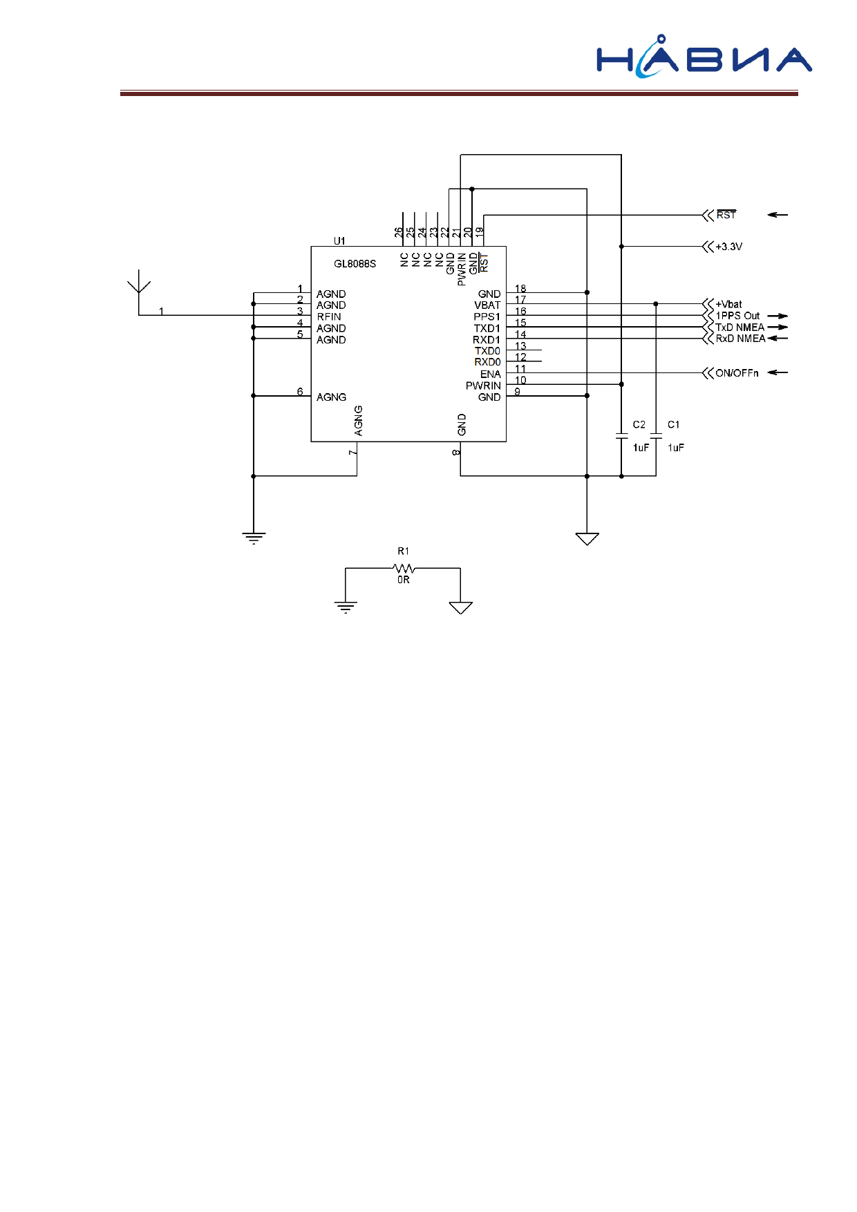
Fig. 5. GL8088s receiver standard connecting diagram.
Figure 5 shows the standard application circuit diagram of GL8088s receiver. The arrows
designate the directions of signals propagation – input signals of the receiver are designated with
arrows "to the receiver", output signals are designated with arrows "from the receiver".
The receiver supply voltage Vdd = 3.0…3.6 V is applied to termination pads 10 and/or 21
(PWRIN) integrated inside the module. In the connecting diagram, this circuit is designated as
+3.3V.
Voltage from the backup battery within the range of Vbat = 2.0…3.6 V must be applied to
termination pad 17 (VBAT). In the application circuit diagram, this circuit is designated as +Vbat.
It is recommended that Vbat be constantly maintained for assurance of built-in RTC clock and
module RAM memory. In addition, the backup battery voltage provides power for the module
internal firmware (the module FW) activation attribute lautch storage register. Use of a backup
battery whose voltage exceeds the module supply voltage is not recommended (Vbat ≤ Vdd).
AT ONLY A FIRST TIME of the module supply voltage Vdd is “ON” following Vbat also
“ON”, be sure to send a low logic level pulse to terminal
i This is
required for selection of operation mode for the integrated microcontroller of the module
(operation or storing of the program in the built-in flash SQI memory), for activation of the
module internal FW and saving of its activation attribute into the storage lautch register. The
pulse duration must be at least 10 ms, the input voltage must not exceed 0.1 V, the source output
capability must be at least 8 mA. At subsequent switching-on of Vdd suppl voltage, sending of
the pulse to input is non-mandatory, since sending of this signal causes eraising of current
time information in RTC, which increases the time of satellites searching and capturing. The
signal states and levels timing diagram at the module connection terminals at Vbat and Vdd
switching-on is shown in figure 6.
11
11 Page | ||
| Páginas | Total 18 Páginas | |
| PDF Descargar | [ Datasheet GL8088s.PDF ] | |
Hoja de datos destacado
| Número de pieza | Descripción | Fabricantes |
| GL8088s | Navigation Receiver Module | HABNA |
| Número de pieza | Descripción | Fabricantes |
| SLA6805M | High Voltage 3 phase Motor Driver IC. |
Sanken |
| SDC1742 | 12- and 14-Bit Hybrid Synchro / Resolver-to-Digital Converters. |
Analog Devices |
|
DataSheet.es es una pagina web que funciona como un repositorio de manuales o hoja de datos de muchos de los productos más populares, |
| DataSheet.es | 2020 | Privacy Policy | Contacto | Buscar |
