|
|
|
PDF 45N03LT Data sheet ( Hoja de datos )
| Número de pieza | 45N03LT | |
| Descripción | PHP45N03LT | |
| Fabricantes | Philips Semiconductors | |
| Logotipo | ||
 1. 30V, 45A, MOSFET - Philips Hay una vista previa y un enlace de descarga de 45N03LT (archivo pdf) en la parte inferior de esta página. Total 8 Páginas | ||
|
No Preview Available !
Philips Semiconductors
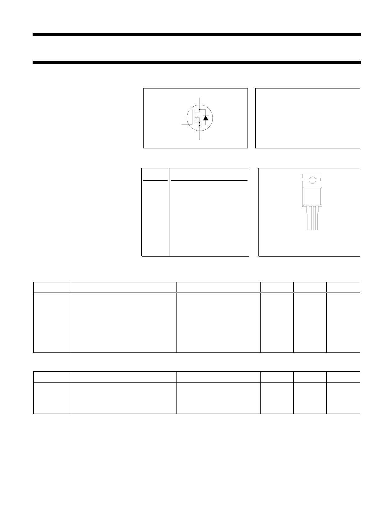
TrenchMOS™ transistor
Logic level FET
Product specification
PHP45N03LT
FEATURES
• ’Trench’ technology
• Very low on-state resistance
• Fast switching
• Stable off-state characteristics
• High thermal cycling performance
• Low thermal resistance
SYMBOL
g
d
s
QUICK REFERENCE DATA
VDSS = 30 V
ID = 45 A
RDS(ON) ≤ 24 mΩ (VGS = 5 V)
RDS(ON) ≤ 21 mΩ (VGS = 10 V)
GENERAL DESCRIPTION
N-channel enhancement mode
logic level field-effect power
transistor in a plastic envelope
using ’trench’ technology. The
device has very low on-state
resistance. It is intended for use in
dc to dc converters and general
purpose switching applications.
The PHP45N03LT is supplied in the
SOT78 (TO220AB) conventional
leaded package.
PINNING
PIN DESCRIPTION
1 gate
2 drain
3 source
tab drain
SOT78 (TO220AB)
tab
1 23
LIMITING VALUES
Limiting values in accordance with the Absolute Maximum System (IEC 134)
SYMBOL PARAMETER
CONDITIONS
VDS
VDGR
±VGS
ID
ID
IDM
Ptot
Tstg, Tj
Drain-source voltage
Drain-gate voltage
Gate-source voltage
Drain current (DC)
Drain current (DC)
Drain current (pulse peak value)
Total power dissipation
Storage & operating temperature
-
RGS = 20 kΩ
-
Tmb = 25 ˚C
Tmb = 100 ˚C
Tmb = 25 ˚C
Tmb = 25 ˚C
-
THERMAL RESISTANCES
SYMBOL
Rth j-mb
Rth j-a
PARAMETER
Thermal resistance junction to
mounting base
Thermal resistance junction to
ambient
CONDITIONS
-
in free air
MIN.
-
-
-
-
-
-
-
- 55
MAX.
30
30
15
45
36
180
86
175
UNIT
V
V
V
A
A
A
W
˚C
TYP.
-
60
MAX.
1.75
-
UNIT
K/W
K/W
November 1997
1
Rev 1.200
1 page 
Philips Semiconductors
TrenchMOS™ transistor
Logic level FET
Product specification
PHP45N03LT
ID / A
60
9528-30
50
Tj / C = 25
175
40
30
20
10
0
0123456
VGS / V
Fig.7. Typical transfer characteristics.
ID = f(VGS) ; conditions: VDS = 25 V; parameter Tj
gfs / S
25
9528-30
20
Tj / C = 25
15 175
10
5
0
0 10 20 30 40 50 60
ID / A
Fig.8. Typical transconductance, Tj = 25 ˚C.
gfs = f(ID); conditions: VDS = 25 V
a
2
30V TrenchMOS
1.5
1
0.5
0
-100
-50
0 50 100 150 200
Tj / C
Fig.9. Normalised drain-source on-state resistance.
a = RDS(ON)/RDS(ON)25 ˚C = f(Tj); ID = 25 A; VGS = 5 V
VGS(TO) / V
2.5
max.
2
typ.
1.5
min.
1
BUK959-60
0.5
0
-100
-50
0 50
Tj / C
100 150 200
Fig.10. Gate threshold voltage.
VGS(TO) = f(Tj); conditions: ID = 1 mA; VDS = VGS
1E-01
Sub-Threshold Conduction
1E-02
1E-03
2% typ 98%
1E-04
1E-05
1E-05
0 0.5 1 1.5 2 2.5
Fig.11. Sub-threshold drain current.
ID = f(VGS); conditions: Tj = 25 ˚C; VDS = VGS
3
C / pF
10000
9528-30
1000
Ciss
Coss
Crss
100
0.1
1 10
VDS / V
100
Fig.12. Typical capacitances, Ciss, Coss, Crss.
C = f(VDS); conditions: VGS = 0 V; f = 1 MHz
November 1997
5
Rev 1.200
5 Page | ||
| Páginas | Total 8 Páginas | |
| PDF Descargar | [ Datasheet 45N03LT.PDF ] | |
Hoja de datos destacado
| Número de pieza | Descripción | Fabricantes |
| 45N03LT | PHP45N03LT | Philips Semiconductors |
| 45N03LTG | P45N03LTG | Niko |
| Número de pieza | Descripción | Fabricantes |
| SLA6805M | High Voltage 3 phase Motor Driver IC. |
Sanken |
| SDC1742 | 12- and 14-Bit Hybrid Synchro / Resolver-to-Digital Converters. |
Analog Devices |
|
DataSheet.es es una pagina web que funciona como un repositorio de manuales o hoja de datos de muchos de los productos más populares, |
| DataSheet.es | 2020 | Privacy Policy | Contacto | Buscar |