|
|
PDF MAX17121 Data sheet ( Hoja de datos )
| Número de pieza | MAX17121 | |
| Descripción | Dual High-Voltage Scan Drivers | |
| Fabricantes | Maxim Integrated Products | |
| Logotipo |  |
|
Hay una vista previa y un enlace de descarga de MAX17121 (archivo pdf) en la parte inferior de esta página. Total 14 Páginas | ||
|
No Preview Available !
19-4936; Rev 0; 9/09
EVAALVUAAILTAIOBNLEKIT
Dual High-Voltage Scan Drivers for TFT LCD
General Description
The MAX17121 includes two high-voltage level-shifting
scan drivers for TFT panel integrated gate logic. Each
scan driver has two channels that switch complementa-
rily. The scan-driver outputs swing from +40V to -30V and
can swiftly drive capacitive loads. In order to save power,
the scan driver’s complementary outputs share the
charge of their capacitive load before they change states.
The MAX17121 is available in a 24-pin, 4mm x 4mm, thin
QFN package with a maximum thickness of 0.8mm for
ultra-thin LCD panels.
Applications
Notebook Computer Displays
LCD Monitor and Small TV Panels
Features
S +40V to -30V Output Swing Range
S Fast Slew Rate for High Capacitive Load
S Load Charge Sharing for Power Saving
S 24-Pin, 4mm x 4mm, Thin QFN Package
Ordering Information
PART
MAX17121ETG+
*EP = Exposed pad.
TEMP RANGE
-40°C to +85°C
PIN-PACKAGE
24 TQFN-EP*
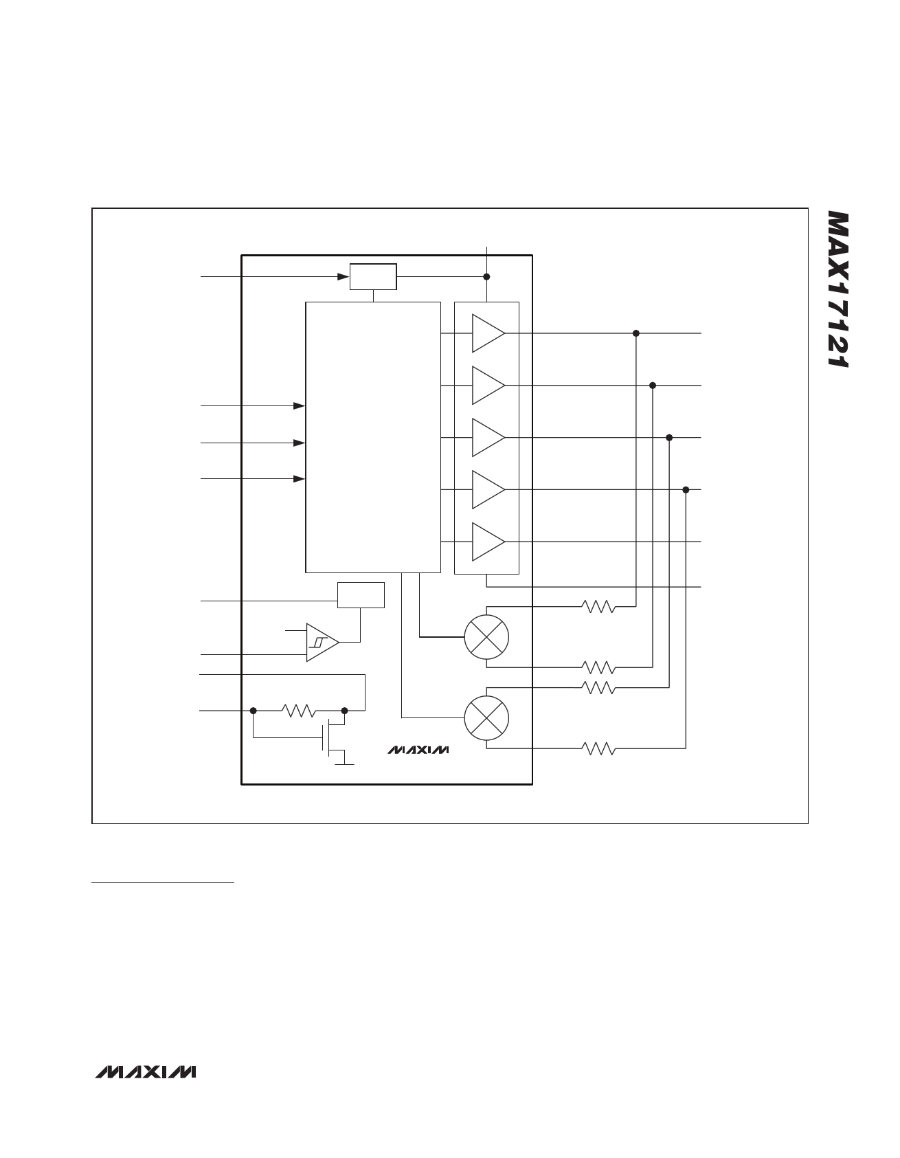
Simplified Operating Circuit
VVON = 25V VVOFF = -15V
TOP VIEW
Pin Configuration
CKVB1
STVP
200I
CKVB2
CKVBCS2
200I
CKVCS2
CKV2
STV
MAX17121
STV
EN
T-CON
CPV1
CPV2
N.C.
N.C.
N.C.
N.C.
VVDD = 3.3V
24 23 22 21 20 19
CKVB1 1
18 VOFF
STVP 2
17 N.C.
CKVB2 3
CKVBCS2 4
MAX17121
16 VDD
15 DISH
CKVCS2 5
*EP
14 GND
CKV2 6
13 N.C.
7 8 9 10 11 12
*EP = EXPOSED PAD
________________________________________________________________ Maxim Integrated Products 1
For pricing, delivery, and ordering information, please contact Maxim Direct at 1-888-629-4642,
or visit Maxim’s website at www.maxim-ic.com.
1 page 
Dual High-Voltage Scan Drivers for TFT LCD
ELECTRICAL CHARACTERISTICS (continued)
(VVDD = VEN = +3.3V, VVON = 25V, VVOFF = -15V, STV = CPV1 = CPV2 = GND, TA = -40NC to +85NC, unless otherwise noted.)
(Note 2)
PARAMETER
CONDITIONS
MIN TYP MAX UNITS
CKVCS_-to-CMVBCS Resistance
STVP Output Low
STVP Output High
STV Rising to STVP Rising
I(CKVCS_-to-CKVBCS) = 10mA
I(STVP) = -20mA
I(STVP) = 20mA
100 I
10 I
35 I
200 ns
STV Falling to STVP Falling
200 ns
STVP Slew Rate Rising
STVP Slew Rate Falling
CPV_ Input Frequency
CL = 4.7nF
CL = 4.7nF
50 V/Fs
50 V/Fs
85 kHz
Input Low Voltage
Input High Voltage
Input Hysteresis
CPV_, STV, EN, 2.2V P VVDD P 3.6V
CPV_, STV, EN, 2.2V P VVDD P 3.6V
CPV_, STV, EN
2.1
0.8 V
V
mV
DISH Low Voltage
-1.5 V
DISH High Voltage
-0.5 V
DISH Hysteresis
mV
DISH Input Impedance
DISH Switch Resistance
DLY Output Current
DLY Sink Current
DLY Enable Threshold
VDISH = -2V
VDISH = -2V
DLY = GND
EN = GND, VDLY = 0.4V
Rising
3
5
1.60
600
500
5
1.70
kI
I
FA
mA
V
Note 1: Guaranteed by design. Not production tested.
Note 2: Limits are 100% production tested at TA = +25NC. Maximum and minimum limits over temperature are guaranteed by
design and characterization.
_______________________________________________________________________________________ 5
5 Page 
Dual High-Voltage Scan Drivers for TFT LCD
VDD UVLO
STV
CPV1
CPV2
LOGIC AND GATE
DRIVER
+
THERMAL
SHUTDOWN
DLY
EN
GND
DSCHG
0.5V
DISH
DELAY
VOFF MAX17121
VON
CKV1
CKVB1
CKV2
CKVB2
STVP
VOFF
CKVCS1
CKVBCS1
CKVCS2
CKVBCS2
Figure 2. Functional Diagram
Detailed Description
The MAX17121 contains two high-voltage level-shifting
scan drivers for active-matrix TFT LCDs. Figure 2 is the
functional diagram.
Undervoltage Lockout on VDD
The undervoltage-lockout (VDD-UVLO) circuit on VDD
compares the input voltage at VDD with the VDD-UVLO
(2V typ) to ensure that the input voltage is high enough
for reliable operation. There is 100mV of hysteresis to
prevent supply transients from causing a restart. When
the VDD voltage is below VDD-UVLO, the scan-driver
outputs are high impedance.
Undervoltage Lockout on VON
The undervoltage-lockout (VON-UVLO) circuit on VON
compares the input voltage at VON with the VON-UVLO
(12V typ) to ensure that the input voltage is high enough
for reliable operation. There is 1V of hysteresis to prevent
supply transients from causing a restart. When the VON
voltage is below VON-UVLO, the scan-driver outputs are
high impedance.
______________________________________________________________________________________ 11
11 Page | ||
| Páginas | Total 14 Páginas | |
| PDF Descargar | [ Datasheet MAX17121.PDF ] | |
Hoja de datos destacado
| Número de pieza | Descripción | Fabricantes |
| MAX1712 | High-Speed / Digitally Adjusted Step-Down Controllers for Notebook CPUs | Maxim Integrated |
| MAX17120 | Triple High-Voltage Scan Driver | Maxim Integrated Products |
| MAX17121 | Dual High-Voltage Scan Drivers | Maxim Integrated Products |
| MAX17122 | Boost-Buck Regulator | Maxim Integrated Products |
| Número de pieza | Descripción | Fabricantes |
| SLA6805M | High Voltage 3 phase Motor Driver IC. |
Sanken |
| SDC1742 | 12- and 14-Bit Hybrid Synchro / Resolver-to-Digital Converters. |
Analog Devices |
|
DataSheet.es es una pagina web que funciona como un repositorio de manuales o hoja de datos de muchos de los productos más populares, |
| DataSheet.es | 2020 | Privacy Policy | Contacto | Buscar |
