|
|
|
PDF AD620 Data sheet ( Hoja de datos )
| Número de pieza | AD620 | |
| Descripción | Low Power Instrumentation Amplifier | |
| Fabricantes | Analog Devices | |
| Logotipo | ||
 1. Datasheet PDF - Instrumentation Amplifier Hay una vista previa y un enlace de descarga de AD620 (archivo pdf) en la parte inferior de esta página. Total 16 Páginas | ||
|
No Preview Available !
a
Low Cost, Low Power
Instrumentation Amplifier
FEATURES
EASY TO USE
Gain Set with One External Resistor
(Gain Range 1 to 1000)
Wide Power Supply Range (؎2.3 V to ؎18 V)
Higher Performance than Three Op Amp IA Designs
Available in 8-Lead DIP and SOIC Packaging
Low Power, 1.3 mA max Supply Current
EXCELLENT DC PERFORMANCE (“B GRADE”)
50 V max, Input Offset Voltage
0.6 V/؇C max, Input Offset Drift
1.0 nA max, Input Bias Current
100 dB min Common-Mode Rejection Ratio (G = 10)
LOW NOISE
9 nV/√Hz, @ 1 kHz, Input Voltage Noise
0.28 V p-p Noise (0.1 Hz to 10 Hz)
EXCELLENT AC SPECIFICATIONS
120 kHz Bandwidth (G = 100)
15 s Settling Time to 0.01%
APPLICATIONS
Weigh Scales
ECG and Medical Instrumentation
Transducer Interface
Data Acquisition Systems
Industrial Process Controls
Battery Powered and Portable Equipment
PRODUCT DESCRIPTION
The AD620 is a low cost, high accuracy instrumentation ampli-
fier that requires only one external resistor to set gains of 1 to
AD620
CONNECTION DIAGRAM
8-Lead Plastic Mini-DIP (N), Cerdip (Q)
and SOIC (R) Packages
RG 1
–IN 2
+IN 3
–VS 4
AD620
TOP VIEW
8 RG
7 +VS
6 OUTPUT
5 REF
1000. Furthermore, the AD620 features 8-lead SOIC and DIP
packaging that is smaller than discrete designs, and offers lower
power (only 1.3 mA max supply current), making it a good fit
for battery powered, portable (or remote) applications.
The AD620, with its high accuracy of 40 ppm maximum
nonlinearity, low offset voltage of 50 µV max and offset drift of
0.6 µV/°C max, is ideal for use in precision data acquisition
systems, such as weigh scales and transducer interfaces. Fur-
thermore, the low noise, low input bias current, and low power
of the AD620 make it well suited for medical applications such
as ECG and noninvasive blood pressure monitors.
The low input bias current of 1.0 nA max is made possible with
the use of Superβeta processing in the input stage. The AD620
works well as a preamplifier due to its low input voltage noise of
9 nV/√Hz at 1 kHz, 0.28 µV p-p in the 0.1 Hz to 10 Hz band,
0.1 pA/√Hz input current noise. Also, the AD620 is well suited
for multiplexed applications with its settling time of 15 µs to
0.01% and its cost is low enough to enable designs with one in-
amp per channel.
30,000
10,000
25,000
20,000
15,000
10,000
5,000
AD620A
RG
3 OP-AMP
IN-AMP
(3 OP-07s)
1,000
100
10
1
TYPICAL STANDARD
BIPOLAR INPUT
IN-AMP
G = 100
AD620 SUPERETA
BIPOLAR INPUT
IN-AMP
0
0 5 10 15 20
SUPPLY CURRENT – mA
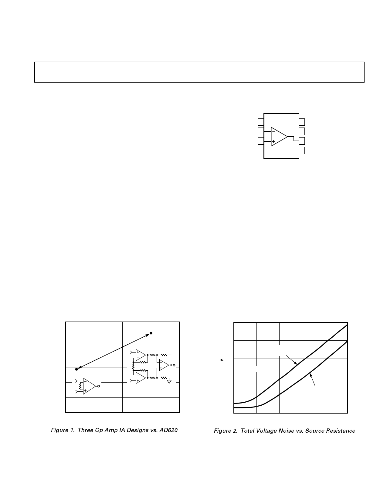
Figure 1. Three Op Amp IA Designs vs. AD620
REV. E
Information furnished by Analog Devices is believed to be accurate and
reliable. However, no responsibility is assumed by Analog Devices for its
use, nor for any infringements of patents or other rights of third parties
which may result from its use. No license is granted by implication or
otherwise under any patent or patent rights of Analog Devices.
0.1
1k
10k 100k 1M
10M
SOURCE RESISTANCE – ⍀
100M
Figure 2. Total Voltage Noise vs. Source Resistance
One Technology Way, P.O. Box 9106, Norwood, MA 02062-9106, U.S.A.
Tel: 781/329-4700
World Wide Web Site: http://www.analog.com
Fax: 781/326-8703
© Analog Devices, Inc., 1999
1 page 
AD620
Typical Characteristics (@ +25؇C, VS = ؎15 V, RL = 2 k⍀, unless otherwise noted)
50
SAMPLE SIZE = 360
40
30
20
2.0
1.5
1.0
0.5
0
–0.5
+IB
–I B
10
0
–80
–40 0
+40
INPUT OFFSET VOLTAGE – V
+80
Figure 3. Typical Distribution of Input Offset Voltage
–1.0
–1.5
–2.0
–75 –25 25 75 125 175
TEMPERATURE – ؇C
Figure 6. Input Bias Current vs. Temperature
50
SAMPLE SIZE = 850
40
30
20
10
0
–1200
–600
0 +600
INPUT BIAS CURRENT – pA
+1200
Figure 4. Typical Distribution of Input Bias Current
2
1.5
1
0.5
0
01 2 34 5
WARM-UP TIME – Minutes
Figure 7. Change in Input Offset Voltage vs.
Warm-Up Time
50
SAMPLE SIZE = 850
40
30
20
10
0
–400
–200
0 +200
INPUT OFFSET CURRENT – pA
+400
Figure 5. Typical Distribution of Input Offset Current
1000
100
GAIN = 1
GAIN = 10
10
GAIN = 100, 1,000
GAIN = 1000
BW LIMIT
1
1 10 100 1k 10k
FREQUENCY – Hz
100k
Figure 8. Voltage Noise Spectral Density vs. Frequency,
(G = 1–1000)
REV. E
–5–
5 Page 
AD620
Make vs. Buy: A Typical Bridge Application Error Budget
The AD620 offers improved performance over “homebrew”
three op amp IA designs, along with smaller size, fewer compo-
nents and 10× lower supply current. In the typical application,
shown in Figure 34, a gain of 100 is required to amplify a bridge
output of 20 mV full scale over the industrial temperature range
of –40°C to +85°C. The error budget table below shows how to
calculate the effect various error sources have on circuit accuracy.
Regardless of the system in which it is being used, the AD620
provides greater accuracy, and at low power and price. In simple
systems, absolute accuracy and drift errors are by far the most
significant contributors to error. In more complex systems with
an intelligent processor, an autogain/autozero cycle will remove all
absolute accuracy and drift errors leaving only the resolution
errors of gain nonlinearity and noise, thus allowing full 14-bit
accuracy.
Note that for the homebrew circuit, the OP07 specifications for
input voltage offset and noise have been multiplied by √2. This
is because a three op amp type in-amp has two op amps at its
inputs, both contributing to the overall input error.
+10V
R = 350⍀
R = 350⍀
R = 350⍀
R = 350⍀
PRECISION BRIDGE TRANSDUCER
RG
499⍀
AD620A
100⍀**
OP07D
10k⍀*
10k⍀**
10k⍀**
10k⍀*
OP07D
REFERENCE
AD620A MONOLITHIC
INSTRUMENTATION
AMPLIFIER, G = 100
SUPPLY CURRENT = 1.3mA MAX
Figure 34. Make vs. Buy
OP07D
10k⍀*
10k⍀*
“HOMEBREW” IN-AMP, G = 100
*0.02% RESISTOR MATCH, 3PPM/؇C TRACKING
**DISCRETE 1% RESISTOR, 100PPM/؇C TRACKING
SUPPLY CURRENT = 15mA MAX
Table I. Make vs. Buy Error Budget
Error Source
AD620 Circuit
Calculation
“Homebrew” Circuit
Calculation
ABSOLUTE ACCURACY at TA = +25°C
Input Offset Voltage, µV
Output Offset Voltage, µV
Input Offset Current, nA
CMR, dB
125 µV/20 mV
1000 µV/100/20 mV
2 nA × 350 Ω/20 mV
110 dB→3.16 ppm, × 5 V/20 mV
(150 µV × √2)/20 mV
((150 µV × 2)/100)/20 mV
(6 nA × 350 Ω)/20 mV
(0.02% Match × 5 V)/20 mV/100
DRIFT TO +85°C
Gain Drift, ppm/°C
Input Offset Voltage Drift, µV/°C
Output Offset Voltage Drift, µV/°C
(50 ppm + 10 ppm) × 60°C
1 µV/°C × 60°C/20 mV
15 µV/°C × 60°C/100/20 mV
Total Absolute Error
100 ppm/°C Track × 60°C
(2.5 µV/°C × √2 × 60°C)/20 mV
(2.5 µV/°C × 2 × 60°C)/100/20 mV
RESOLUTION
Gain Nonlinearity, ppm of Full Scale
40 ppm
Typ 0.1 Hz–10 Hz Voltage Noise, µV p-p 0.28 µV p-p/20 mV
Total Drift Error
40 ppm
(0.38 µV p-p × √2)/20 mV
Total Resolution Error
Grand Total Error
G = 100, VS = ± 15 V.
(All errors are min/max and referred to input.)
Error, ppm of Full Scale
AD620
Homebrew
16,250
14,500
14,118
14,791
17,558
13,600
13,000
14,450
17,050
14,140
141,14
14,154
14,662
10,607
10,150
14,153
10,500
11,310
16,000
10,607
10,150
16,757
10,140
13,127
101,67
28,134
REV. E
–11–
11 Page | ||
| Páginas | Total 16 Páginas | |
| PDF Descargar | [ Datasheet AD620.PDF ] | |
Hoja de datos destacado
| Número de pieza | Descripción | Fabricantes |
| AD620 | Low Power Instrumentation Amplifier | Analog Devices |
| AD621 | Low Drift/ Low Power Instrumentation Amplifier | Analog Devices |
| AD622 | Low Cost Instrumentation Amplifier | Analog Devices |
| AD623 | Low Cost Instrumentation Amplifier | Analog Devices |
| Número de pieza | Descripción | Fabricantes |
| SLA6805M | High Voltage 3 phase Motor Driver IC. |
Sanken |
| SDC1742 | 12- and 14-Bit Hybrid Synchro / Resolver-to-Digital Converters. |
Analog Devices |
|
DataSheet.es es una pagina web que funciona como un repositorio de manuales o hoja de datos de muchos de los productos más populares, |
| DataSheet.es | 2020 | Privacy Policy | Contacto | Buscar |