|
|
|
PDF MCP6042 Data sheet ( Hoja de datos )
| Número de pieza | MCP6042 | |
| Descripción | Rail-to-Rail Input/Output Op Amps | |
| Fabricantes | Microchip Technology | |
| Logotipo | ||
Hay una vista previa y un enlace de descarga de MCP6042 (archivo pdf) en la parte inferior de esta página. Total 30 Páginas | ||
|
No Preview Available !
MCP6041/2/3/4
600 nA, Rail-to-Rail Input/Output Op Amps
Features
• Low Quiescent Current: 600 nA/amplifier (typical)
• Rail-to-Rail Input/Output
• Gain Bandwidth Product: 14 kHz (typical)
• Wide Supply Voltage Range: 1.4V to 6.0V
• Unity Gain Stable
• Available in Single, Dual, and Quad
• Chip Select (CS) with MCP6043
• Available in 5-lead and 6-lead SOT-23 Packages
• Temperature Ranges:
- Industrial: -40°C to +85°C
- Extended: -40°C to +125°C
Applications
• Toll Booth Tags
• Wearable Products
• Temperature Measurement
• Battery Powered
Design Aids
• SPICE Macro Models
•F ilterLab® Software
• MAPS (Microchip Advanced Part Selector)
• Analog Demonstration and Evaluation Boards
• Application Notes
Related Devices
• MCP6141/2/3/4: G = +10 Stable Op Amps
Typical Application
IDD
1.4V
to
6.0V
10
100 k
MCP604X
VDD
VOUT
1M
IDD = ---1--0V--DV---D/-V--–--V--O-1--U-0-T-----
High Side Battery Current Sensor
Description
The MC P6041/2/3/4 fa mily of operational amplifiers
(op amps) from Microchip Technology Inc. operate with
a single supply voltage as low as 1.4V, while drawing
less tha n 1 µA (m aximum) of q uiescent current p er
amplifier. These devices are also designed to su pport
rail-to-rail input and output operation. This combination
of fea tures s upports bat tery-powered and port able
applications.
The MCP6041/2/3/4 amplifiers have a gain-bandwidth
product o f 14 kHz (ty pical) and are u nity g ain st able.
These specifications make these op amps appropriate
for low frequency applications, such as battery current
monitoring and sensor conditioning.
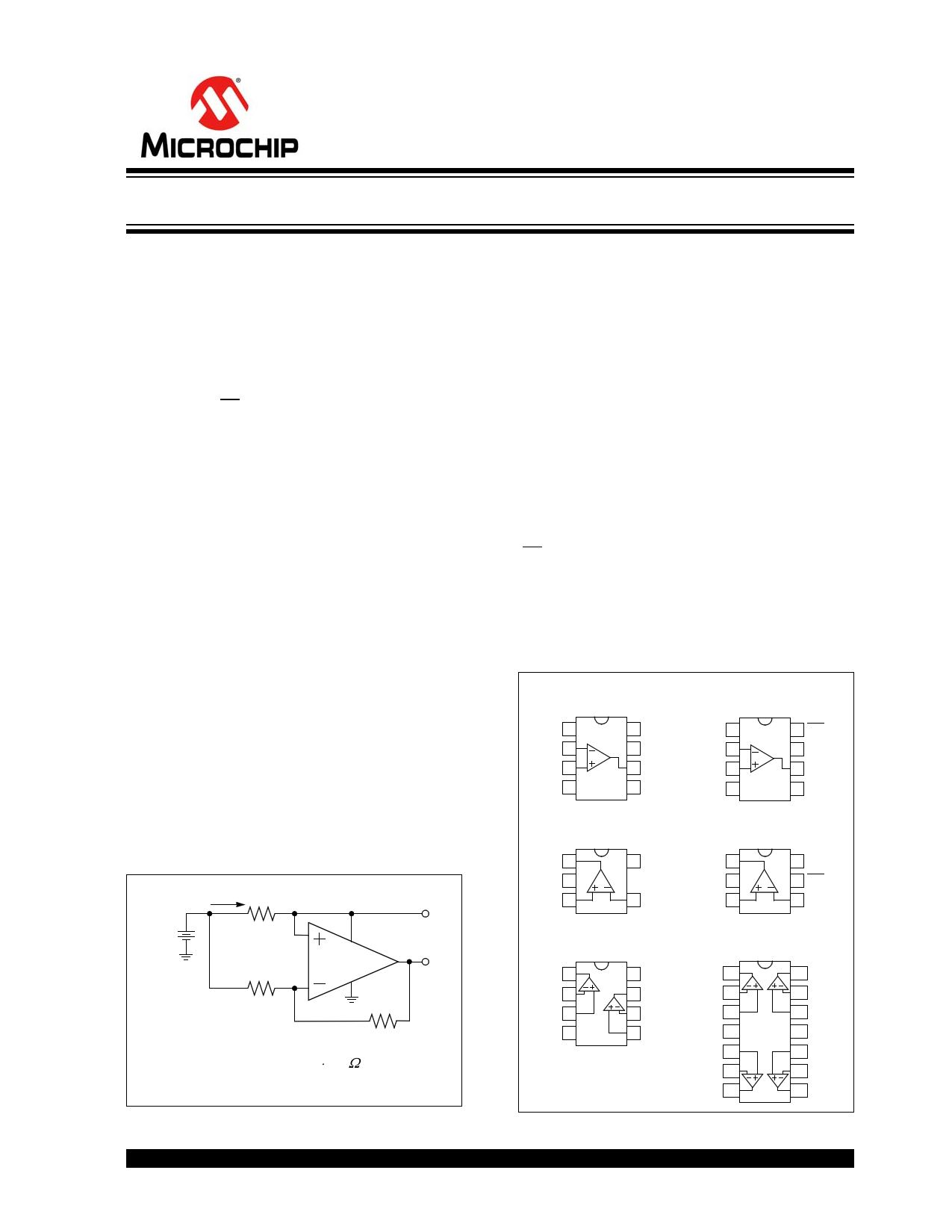
The M CP6041/2/3/4 family ope rational am plifiers a re
offered in s ingle (M CP6041), s ingle w ith C hip Se lect
(CS) (M CP6043), d ual (MC P6042), and qua d
(MCP6044) configurations. Th e MCP6041 de vice i s
available in th e 5-l ead SOT -23 p ackage, a nd th e
MCP6043 d evice is av ailable i n th e 6 -lead SO T-23
package.
Package Types
MCP6041
PDIP, SOIC, MSOP
MCP6043
PDIP, SOIC, MSOP
NC 1
VIN– 2
VIN+ 3
VSS 4
8 NC
7 VDD
6 VOUT
5 NC
NC 1
VIN– 2
VIN+ 3
VSS 4
8 CS
7 VDD
6 VOUT
5 NC
MCP6041
SOT-23-5
VOUT 1
VSS 2
VIN+ 3
5 VDD
4 VIN–
MCP6043
SOT-23-6
VOUT 1
VSS 2
VIN+ 3
6 VDD
5 CS
4 VIN–
MCP6042
PDIP, SOIC, MSOP
MCP6044
PDIP, SOIC, TSSOP
VOUTA 1
VINA– 2
VINA+ 3
VSS 4
8 VDD VOUTA 1
7 VOUTB VINA– 2
6 VINB– VINA+ 3
5 VINB+ VDD 4
VINB+ 5
VINB– 6
VOUTB 7
14 VOUTD
13 VIND–
12 VIND+
11 VSS
10 VINC+
9 VINC–
8 VOUTC
2001-2013 Microchip Technology Inc.
DS21669D-page 1
http://www.Datasheet4U.com
1 page 
MCP6041/2/3/4
2.0 TYPICAL PERFORMANCE CURVES
Note:
The graphs and tables provided following this note are a statistical summary based on a limited number of
samples and are provided for informational purposes only. The performance characteristics listed herein are
not tes ted or guaranteed. In some gra phs or t ables, the da ta pre sented may be ou tside the sp ecified
operating range (e.g., outside specified power supply range) and therefore outside the warranted range.
Note: Unless otherwise indicated, TA = +25°C, VDD = +1.4V to +6.0V, VSS = GND, VCM = VDD/2, VOUT VDD/2,
VL = VDD/2, RL = 1 M to VL, and CL = 60 pF.
10%
9%
8%
7%
1124 Samples
VDD = 1.4V and 5.5V
VCM = VSS
6%
5%
4%
3%
2%
1%
0%
-3
-2 -1 0 1
Input Offset Voltage (mV)
2
3
18%
16%
14%
12%
10%
8%
6%
4%
2%
0%
-32
245 Samples
1 Representative Lot
TA = +85°C to +125°C
VDD = 1.4V
VCM = VSS
-28 -24 -20 -16 -12 -8 -4 0
Input Offset Voltage Drift (µV/°C)
4
FIGURE 2-1:
Input Offset Voltage.
FIGURE 2-4:
Input Offset Voltage Drift
with TA = +85°C to +125°C and VDD =1 .4V.
12%
11%
10%
9%
8%
1124 Samples
TA = -40°C to +85°C
VDD = 1.4V
VCM = VSS
7%
6%
5%
4%
3%
2%
1%
0%
-10 -8 -6 -4 -2 024
68
Input Offset Voltage Drift (µV/°C)
10
FIGURE 2-2:
Input Offset Voltage Drift
with TA = -40°C to +85°C.
24%
22%
20%
18%
16%
14%
239 Samples
1 Representative Lot
TA = +85°C to +125°C
VDD = 5.5V
VCM = VSS
12%
10%
8%
6%
4%
2%
0%
-32 -28 -24 -20 -16 -12 -8 -4 0
Input Offset Voltage Drift (µV/°C)
4
FIGURE 2-5:
Input Offset Voltage Drift
with TA = +25°C to +125°C and VDD =5 .5V.
2000
1500
1000
500
0
-500
-1000
-1500
-2000
VDD = 1.4V
Representative Part
TA = +125°C
TA = +85°C
TA = +25°C
TA = -40°C
Common Mode Input Voltage (V)
FIGURE 2-3:
Input Offset Voltage vs.
Common Mode Input Voltage with VDD = 1.4V.
2000
1500
1000
500
0
-500
-1000
-1500
-2000
VDD = 5.5V
Representative Part
TA = +125°C
TA = +85°C
TA = +25°C
TA = -40°C
Common Mode Input Voltage (V)
FIGURE 2-6:
Input Offset Voltage vs.
Common Mode Input Voltage with VDD = 5.5V.
2001-2013 Microchip Technology Inc.
DS21669D-page 5
5 Page 
MCP6041/2/3/4
3.0 PIN DESCRIPTIONS
Descriptions of the pins are listed in Table 3-1.
TABLE 3-1: PIN FUNCTION TABLE
MCP6041
MCP6042
MCP6043
MCP6044
PDIP,
SOIC,
MSOP
61
24
33
75
——
——
——
——
——
——
42
——
——
——
——
1, 5, 8
SOT-23-5
—
PDIP,
SOIC,
MSOP
1
2
3
8
5
6
7
—
—
—
4
—
—
—
—
—
PDIP,
SOIC,
MSOP
6
2
3
7
—
—
—
—
—
—
4
—
—
—
8
1, 5
SOT-23-6
1
4
3
6
—
—
—
—
—
—
2
—
—
—
5
—
PDIP,
SOIC,
TSSOP
1
2
3
4
5
6
7
8
9
10
11
12
13
14
—
—
Symbol
Description
VOUT,V OUTA Analog Output (op amp A)
VIN–, VINA– Inverting Input (op amp A)
VIN+, VINA+ Non-inverting Input (op amp A)
VDD Positive Power Supply
VINB+ Non-inverting Input (op amp B)
VINB– Inverting Input (op amp B)
VOUTB Analog Output (op amp B)
VOUTC Analog Output (op amp C)
VINC– Inverting Input (op amp C)
VINC+ Non-inverting Input (op amp C)
VSS Negative Power Supply
VIND+ Non-inverting Input (op amp D)
VIND– Inverting Input (op amp D)
VOUTD Analog Output (op amp D)
CS Chip Select
NC No Internal Connection
3.1 Analog Outputs
The output pins are low-impedance voltage sources.
3.2 Analog Inputs
The non-inverting and inverting inputs are high-imped-
ance CMOS inputs with low bias currents.
3.3 Chip Select Digital Input
This is a CMOS, Schmitt-triggered input that places the
part into a low power mode of operation.
3.4 Power Supply Pins
The p ositive power s upply pin (V DD) is 1 .4V t o 6. 0V
higher than the negative power supply pin (VSS). For
normal o peration, t he o ther pin s a re a t vo ltages
between VSS and VDD.
Typically, the se p arts are us ed i n a single (po sitive)
supply configuration. In this case, VSS is connected to
ground a nd VDD is co nnected to the supply. VDD wi ll
need bypass capacitors.
2001-2013 Microchip Technology Inc.
DS21669D-page 11
11 Page | ||
| Páginas | Total 30 Páginas | |
| PDF Descargar | [ Datasheet MCP6042.PDF ] | |
Hoja de datos destacado
| Número de pieza | Descripción | Fabricantes |
| MCP604 | 2.7V to 5.5V Single Supply CMOS Op Amps | Microchip Technology |
| MCP604-I | 2.7V to 5.5V Single Supply CMOS Op Amps | Microchip Technology |
| MCP604-IOT | 2.7V to 5.5V Single Supply CMOS Op Amps | Microchip Technology |
| MCP604-IP | 2.7V to 5.5V Single Supply CMOS Op Amps | Microchip Technology |
| Número de pieza | Descripción | Fabricantes |
| SLA6805M | High Voltage 3 phase Motor Driver IC. |
Sanken |
| SDC1742 | 12- and 14-Bit Hybrid Synchro / Resolver-to-Digital Converters. |
Analog Devices |
|
DataSheet.es es una pagina web que funciona como un repositorio de manuales o hoja de datos de muchos de los productos más populares, |
| DataSheet.es | 2020 | Privacy Policy | Contacto | Buscar |