|
|
|
PDF IRF540 Data sheet ( Hoja de datos )
| Número de pieza | IRF540 | |
| Descripción | Power MOSFET ( Transistor ) | |
| Fabricantes | Vishay | |
| Logotipo | ||
 1. 100V, Power MOSFET - IR Hay una vista previa y un enlace de descarga de IRF540 (archivo pdf) en la parte inferior de esta página. Total 9 Páginas | ||
|
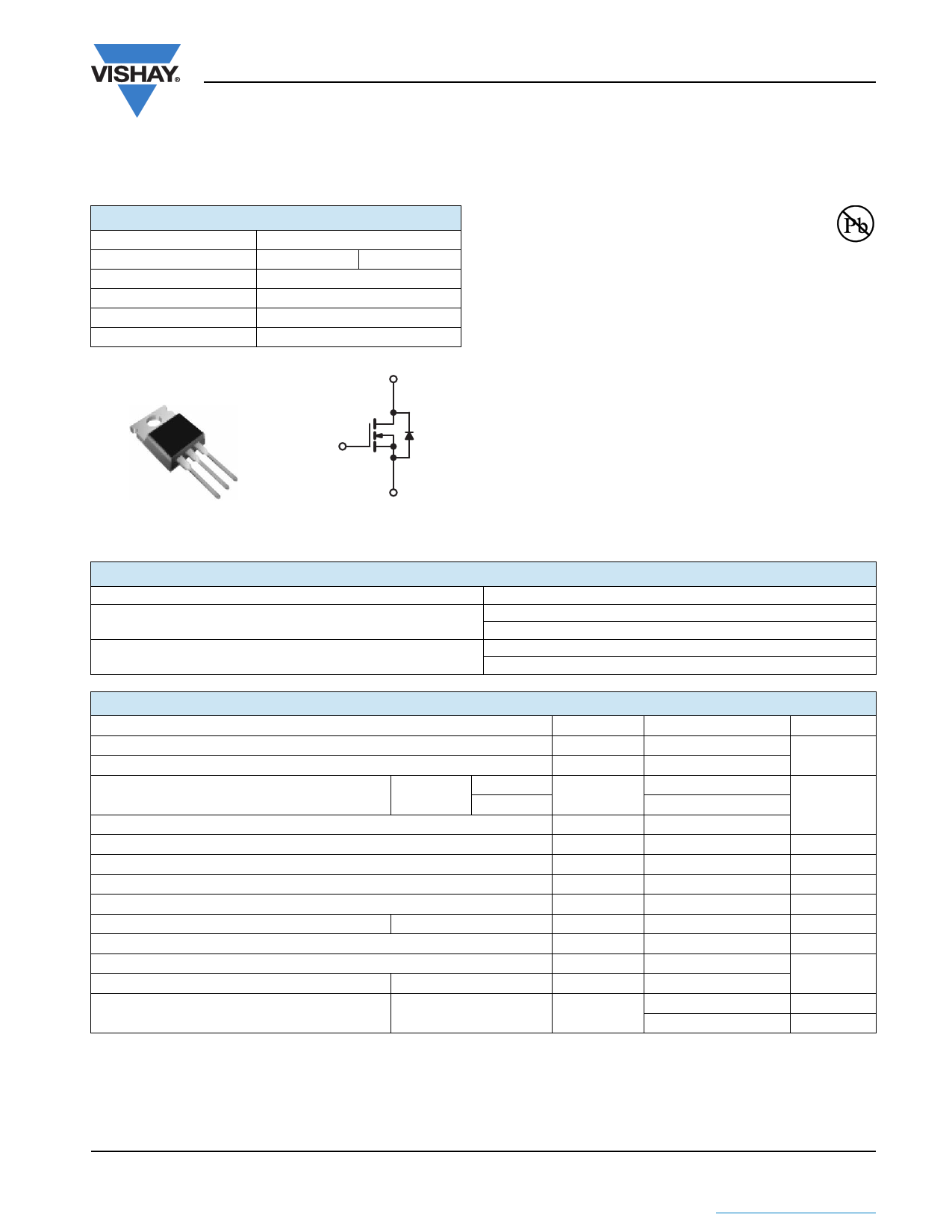
No Preview Available !
Power MOSFET
IRF540, SiHF540
Vishay Siliconix
PRODUCT SUMMARY
VDS (V)
RDS(on) ()
Qg (Max.) (nC)
Qgs (nC)
Qgd (nC)
Configuration
100
VGS = 10 V
72
11
32
Single
0.077
TO-220AB
D
S
D
G
G
S
N-Channel MOSFET
ORDERING INFORMATION
Package
Lead (Pb)-free
SnPb
FEATURES
• Dynamic dV/dt Rating
• Repetitive Avalanche Rated
• 175 °C Operating Temperature
•F ast Switching
• Ease of Paralleling
• Simple Drive Requirements
• Compliant to RoHS Directive 2002/95/EC
Available
RoHS*
COMPLIANT
DESCRIPTION
Third generation Power MOSFETs from Vishay provide the
designer with the best combi nation of fast swi tching,
ruggedized device des ign, low on -resistance a nd
cost-effectiveness.
The TO-220AB package is univers ally preferred for all
commercial-industrial app lications at powe r dissipation
levels to approximately 50 W. The low thermal resistance
and low package c ost of th e TO- 220AB con tribute to its
wide acceptance throughout the industry.
TO-220AB
IRF540PbF
SiHF540-E3
IRF540
SiHF540
ABSOLUTE MAXIMUM RATINGS (TC = 25 °C, unless otherwise noted)
PARAMETER S
YMBOL
Drain-Source Voltage
Gate-Source Voltage
Continuous Drain Current
Pulsed Drain Currenta
Linear Derating Factor
VGS at 10 V
TC = 25 °C
TC = 100 °C
VDS
VGS ±
ID
IDM 110
Single Pulse Avalanche Energyb
Repetitive Avalanche Currenta
Repetitive Avalanche Energya
Maximum Power Dissipation
Peak Diode Recovery dV/dtc
TC = 25 °C
EAS
IAR
EAR
PD
dV/dt 5.5
Operating Junction and Storage Temperature Range
Soldering Recommendations (Peak Temperature)
for 10 s
TJ, Tstg
Mounting Torque
6-32 or M3 screw
Notes
a. Repetitive rating; pulse width limited by maximum junction temperature (see fig. 11).
b. VDD = 25 V, starting TJ = 25 °C, L = 440 μH, Rg = 25 , IAS = 28 A (see fig. 12).
c. ISD 28 A, dI/dt 170 A/μs, VDD VDS, TJ 175 °C.
d. 1.6 mm from case.
LIMIT
100
20
28
20
1.0
230
28
15
150
- 55 to + 175
300d
10 lbf
1.1
UNIT
V
A
W/°C
mJ
A
mJ
W
V/ns
°C
· in
N·m
* Pb containing terminations are not RoHS compliant, exemptions may apply
Document Number: 91021
S11-0510-Rev. B, 21-Mar-11
www
.vishay.com
1
This datasheet is subject to change without notice.
THE PRODUCT DESCRIBED HEREIN AND THIS DATASHEET ARE SUBJECT TO SPECIFIC DISCLAIMERS, SET FORTH AT www.vishay.com/doc?91000
http://www.Datasheet4U.com
1 page 
30
25
20
15
10
5
0
25
91021_09
50 75 100 125 150
TC, Case Temperature (°C)
175
Fig. 9 - Maximum Drain Current vs. Case Temperature
IRF540, SiHF540
Vishay Siliconix
VDS
VGS
RG
RD
D.U.T.
10 V
Pulse width ≤ 1 µs
Duty factor ≤ 0.1 %
+- VDD
Fig. 10a - Switching Time Test Circuit
VDS
90 %
10 %
VGS
td(on) tr
td(off) tf
Fig. 10b - Switching Time Waveforms
10
1
0 − 0.5
0.2
0.1 0.1
0.05
0.02
0.01
10-2
10-5
91021_11
Single Pulse
(Thermal Response)
10-4
10-3
10-2
0.1
t1, Rectangular Pulse Duration (s)
PDM
t1
t2
Notes:
1. Duty Factor, D = t1/t2
2. Peak Tj = PDM x ZthJC + TC
1 10
Fig. 11 - Maximum Effective Transient Thermal Impedance, Junction-to-Case
Document Number: 91021
S11-0510-Rev. B, 21-Mar-11
www
.vishay.com
5
This datasheet is subject to change without notice.
THE PRODUCT DESCRIBED HEREIN AND THIS DATASHEET ARE SUBJECT TO SPECIFIC DISCLAIMERS, SET FORTH AT www.vishay.com/doc?91000
5 Page | ||
| Páginas | Total 9 Páginas | |
| PDF Descargar | [ Datasheet IRF540.PDF ] | |
Hoja de datos destacado
| Número de pieza | Descripción | Fabricantes |
| IRF540 | Power MOSFET ( Transistor ) | Vishay |
| IRF540 | N-Channel Power MOSFETs | Harris |
| IRF540 | N-Channel MOSFET Transistor | Inchange Semiconductor |
| IRF540 | N-channel TrenchMOS transistor | NXP Semiconductors |
| Número de pieza | Descripción | Fabricantes |
| SLA6805M | High Voltage 3 phase Motor Driver IC. |
Sanken |
| SDC1742 | 12- and 14-Bit Hybrid Synchro / Resolver-to-Digital Converters. |
Analog Devices |
|
DataSheet.es es una pagina web que funciona como un repositorio de manuales o hoja de datos de muchos de los productos más populares, |
| DataSheet.es | 2020 | Privacy Policy | Contacto | Buscar |