No Preview Available !

MCP19114/5
Digitally Enhanced Power Analog Synchronous Low-Side PWM Controller
Features
• Input Voltage: 4.5V to 42V
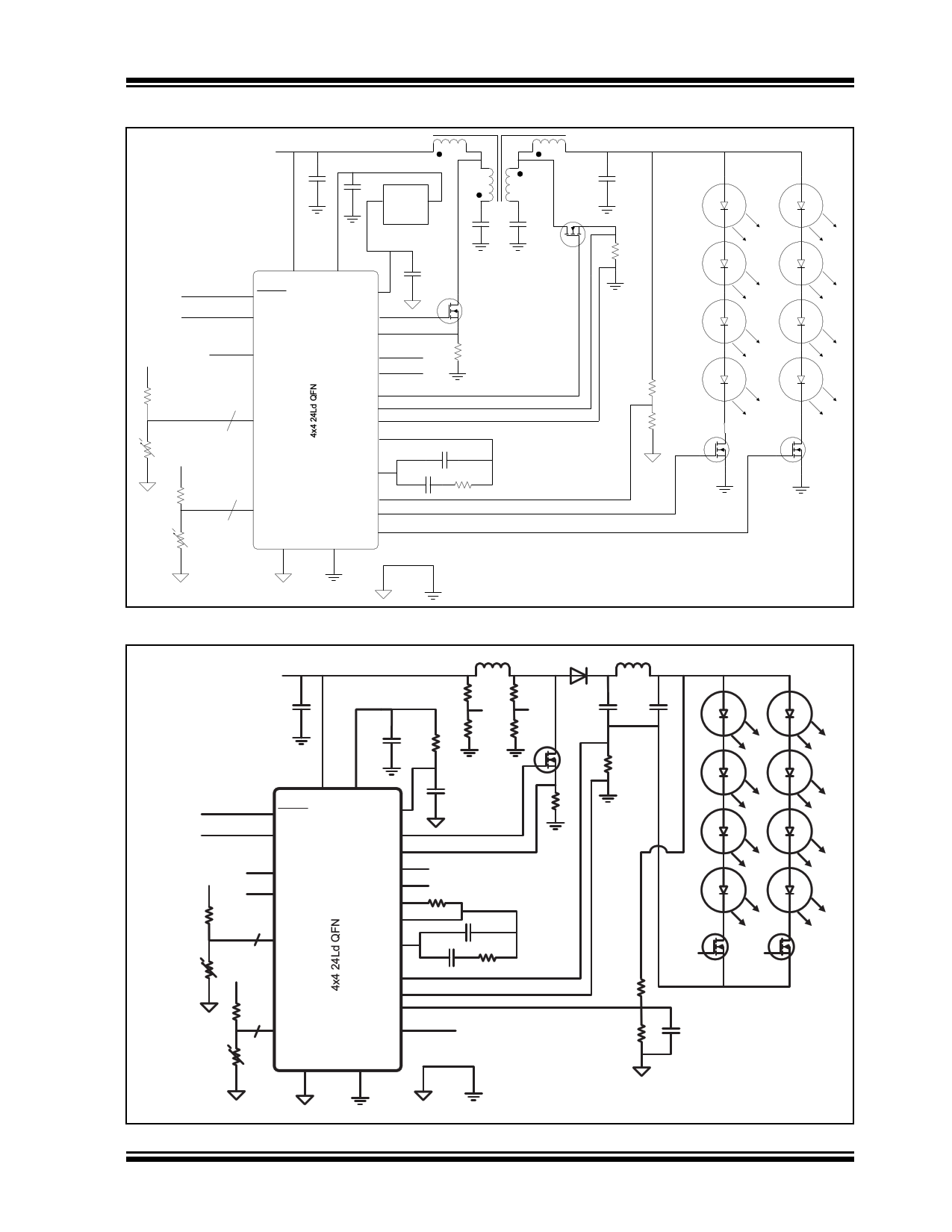
• Can be Configured with Multiple Topologies
Including but not Limited to:
- Flyback
- Ćuk
- Boost
- SEPIC (Single-Ended Primary-Inductor
Converter)
• Capable of Quasi-Resonant or Fixed-Frequency
Operation
• Low Quiescent Current: 5 mA Typical
• Low Sleep Current: 30 µA Typical
• Low-Side Gate Drivers:
- +5V gate drive
- 0.5A sink/source current
- +10V gate drive
- 1A sink/source current
• Peak Current Mode Control
• Differential Remote Output Sense
• Multiple Output Systems:
- Master or Slave
• AEC-Q100 Qualified
• Configurable Parameters:
- VREF, Precision IOUT/VOUT Set Point (DAC)
- Input Undervoltage Lockout (UVLO)
- Input Overvoltage Lockout (OVLO)
- Detection and protection
- Primary current leading edge blanking (0,
50 ns, 100 ns and 200 ns)
- Gate drive dead time (16 ns to 256 ns)
- Fixed switching frequency range: 31.25 kHz
to 2.0 MHz
- Slope compensation
- Quasi-resonant configuration with built-in
comparator and programmable offset voltage
adjustment
- Primary current offset adjustment
- Configurable GPIO pin options
• Integrated Low-Side Differential Current Sense
Amplifier
• ±5% Current Regulation
• Thermal Shutdown
Microcontroller Features
• Precision 8 MHz Internal Oscillator Block:
- Factory-calibrated to ±1%, typical
• Interrupt-Capable
- Firmware
- Interrupt-on-change pins
• Only 35 Instructions to Learn
• 4096 Words On-Chip Program Memory
• High-Endurance Flash:
- 100,000 write Flash endurance
- Flash retention: >40 years
• Watchdog Timer (WDT) with Independent
Oscillator for Reliable Operation
• Programmable Code Protection
• In-Circuit Serial Programming™ (ICSP™) via Two
Pins
• Eight I/O Pins and One Input-Only Pin
- Two open-drain pins
• Analog-to-Digital Converter (ADC):
- 10-bit resolution
- Five external channels
• Timer0: 8-bit Timer/Counter with 8-bit Prescaler
• Enhanced Timer1:
- 16-bit timer with prescaler
- Two selectable clock sources
• Timer2: 8-Bit Timer with Prescaler
- 8-bit period register
• I2CTM Communication:
- 7-bit address masking
- Two dedicated address registers
2014-2015 Microchip Technology Inc.
DS20005281B-page 1

MCP19114/5
TABLE 2: 28-PIN SUMMARY
Basic
Additional
GPA0
GPA1
1 Y AN0
2 Y AN1
—
—
— IOC Y
— IOC Y
— Analog/Digital Debug Output(1)
— Sync Signal In/Out(2)
GPA2 3 Y AN2 T0CKI — IOC Y
INT
—
—
GPA3
5 Y AN3
—
— IOC Y
—
—
GPA5
8N
—
—
— IOC(4) Y(5)
MCLR
Test Enable Input
GPA6
7N
—
—
— IOC Y
—
Dual Capture/Single
Compare1 Input
GPA7
6N
—
— SCL IOC N
—
—
GPB0 10 N
—
— SDA IOC N
—
GPB1 26 Y AN4
—
— IOC Y
—
GPB4
4 Y AN5
—
— IOC Y ICSPDAT
—
VREF2(3)
—
GPB5 27 Y AN6
—
— IOC Y ICSPCLK
—
GPB6 28 Y AN7
—
— IOC Y
—
—
GPB7 9 Y
—
—
— IOC Y
—
Single Compare2 Input
DESATP/ 12 N
—
—
—
—
—
ISOUT
DESATN 11 N
—
—
—
—
—
ISP
13 N
—
—
—
—
Y
—
—
—
DESATOPuintppuutt(6o)r ISOUT
DESAT Negative Input
Current Sense Amplifier
Noninverting Input
ISN 14 N — — — — —
—
Current Sense Amplifier
Inverting Input
IP
15 N
—
—
—
—
—
AGND
16 N
—
—
—
—
—
PGND
17 N
—
—
—
—
—
SDRV 18 N
—
—
—
—
—
—
AGND
PGND
—
Primary Input Current Sense
Small Signal Ground
Large Signal Ground
Secondary LS Gate Drive
Output
PDRV 19 N
—
—
—
—
—
— Primary LS Gate Drive Output
VDR
VDD
VIN
VS
IFB
ICOMP
Note 1:
20 N
—
—
—
—
—
21 N
—
—
—
—
—
22 N
—
—
—
—
—
23 N
—
—
—
—
—
VDR Gate Drive Supply Voltage
VDD
VDD Output
VIN Input Supply Voltage
— Output Voltage Sense
24 N
—
—
—
—
—
— Error Amplifier Feedback input
25 N
—
—
—
—
—
—
Error Amplifier Output
The Analog/Digital Debug Output is selected through the control of the ABECON register.
2: Selected when functioning as master or slave by proper configuration of the MSC<1:0> bits in the
MODECON register.
3: VREF2 output selected when configured as master by proper configuration of the MSC<1:0> bits in the
MODECON register.
4: The IOC is disabled when MCLR is enabled.
5: Weak pull-up always enabled when MCLR is enabled, otherwise the pull-up is under user control.
6: When RFB of MODECON<6> = 0, the internal feedback resistor is enabled allow with DESATP input.
When RFB = 1, ISOUT is enabled.
2014-2015 Microchip Technology Inc.
DS20005281B-page 5


