|
|
|
PDF LMR12010 Data sheet ( Hoja de datos )
| Número de pieza | LMR12010 | |
| Descripción | 1A Step-Down Voltage Regulator | |
| Fabricantes | National Semiconductor | |
| Logotipo | ||
Hay una vista previa y un enlace de descarga de LMR12010 (archivo pdf) en la parte inferior de esta página. Total 16 Páginas | ||
|
No Preview Available !
LMR12010
September 29, 2011
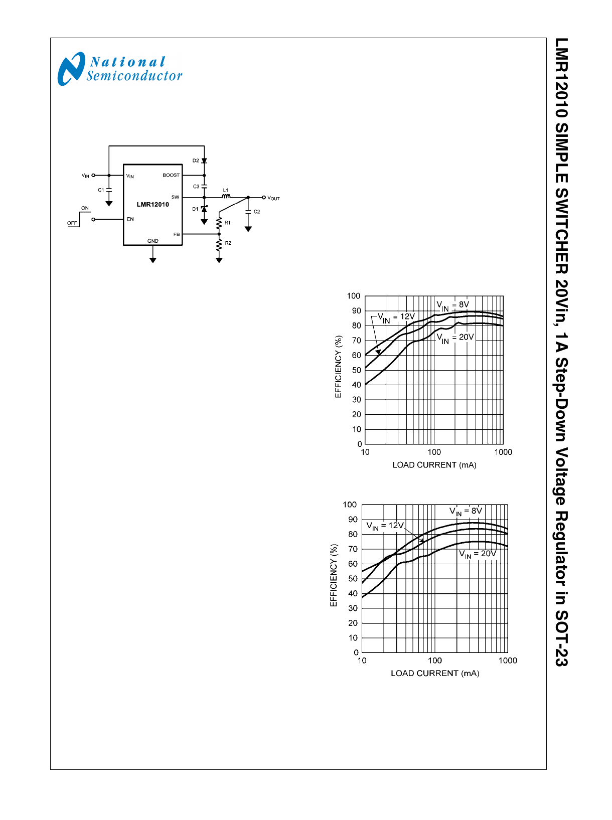
SIMPLE SWITCHER® 20Vin, 1A Step-Down Voltage
Regulator in SOT-23
Applications
■ Point-of-Load Conversions from 3.3V, 5V, and 12V Rails
■ Space Constrained Applications
■ Battery Powered Equipment
■ Industrial Distributed Power Applications
■ Power Meters
■ Portable Hand-Held Instruments
30166501
Features
■ Input voltage range of 3V to 20V
■ Output voltage range of 0.8V to 17V
■ Output current up to 1A
■ 1.6MHz (LMR12010X) and 3 MHz (LMR12010Y)
switching frequencies
■ Low shutdown Iq, 30 nA typical
■ Internal soft-start
■ Internally compensated
■ Current-Mode PWM operation
■ Thermal shutdown
■ Thin SOT23-6 package (2.97 x 1.65 x 1mm)
■ Fully enabled for WEBENCH® Power Designer
System Performance
Efficiency vs Load Current - "X" VOUT = 5V
Performance Benefits
■ Extremely easy to use
■ Tiny overall solution reduces system cost
30166536
Efficiency vs Load Current - "Y" VOUT = 5V
WEBENCH® is a registered trademark of National Semiconductor Corp.
© 2011 National Semiconductor Corporation 301665
30166534
www.national.com
Free Datasheet http://www.datasheet4u.com/
1 page 
Oscillator Frequency vs Temperature - "X"
Oscillator Frequency vs Temperature - "Y"
30166527
Current Limit vs Temperature
VIN = 5V
30166528
Current Limit vs Temperature
VIN = 20V
VFB vs Temperature
30166529
RDSON vs Temperature
30166547
30166533
5
30166530
www.national.com
Free Datasheet http://www.datasheet4u.com/
5 Page 
transient is provided mainly by the output capacitor. The out-
put ripple of the converter is:
When using MLCCs, the ESR is typically so low that the ca-
pacitive ripple may dominate. When this occurs, the output
ripple will be approximately sinusoidal and 90° phase shifted
from the switching action. Given the availability and quality of
MLCCs and the expected output voltage of designs using the
LMR12010, there is really no need to review any other ca-
pacitor technologies. Another benefit of ceramic capacitors is
their ability to bypass high frequency noise. A certain amount
of switching edge noise will couple through parasitic capaci-
tances in the inductor to the output. A ceramic capacitor will
bypass this noise while a tantalum will not. Since the output
capacitor is one of the two external components that control
the stability of the regulator control loop, most applications will
require a minimum at 10 µF of output capacitance. Capaci-
tance can be increased significantly with little detriment to the
regulator stability. Like the input capacitor, recommended
multilayer ceramic capacitors are X7R or X5R. Again, verify
actual capacitance at the desired operating voltage and tem-
perature.
Check the RMS current rating of the capacitor. The RMS cur-
rent rating of the capacitor chosen must also meet the follow-
ing condition:
CATCH DIODE
The catch diode (D1) conducts during the switch off-time. A
Schottky diode is recommended for its fast switching times
and low forward voltage drop. The catch diode should be
chosen so that its current rating is greater than:
ID1 = IO x (1-D)
The reverse breakdown rating of the diode must be at least
the maximum input voltage plus appropriate margin. To im-
prove efficiency choose a Schottky diode with a low forward
voltage drop.
BOOST DIODE
A standard diode such as the 1N4148 type is recommended.
For VBOOST circuits derived from voltages less than 3.3V, a
small-signal Schottky diode is recommended for greater effi-
ciency. A good choice is the BAT54 small signal diode.
BOOST CAPACITOR
A ceramic 0.01µF capacitor with a voltage rating of at least
6.3V is sufficient. The X7R and X5R MLCCs provide the best
performance.
OUTPUT VOLTAGE
The output voltage is set using the following equation where
R2 is connected between the FB pin and GND, and R1 is
connected between VO and the FB pin. A good value for R2
is 10kΩ.
PCB Layout Considerations
When planning layout there are a few things to consider when
trying to achieve a clean, regulated output. The most impor-
tant consideration when completing the layout is the close
coupling of the GND connections of the CIN capacitor and the
catch diode D1. These ground ends should be close to one
another and be connected to the GND plane with at least two
through-holes. Place these components as close to the IC as
possible. Next in importance is the location of the GND con-
nection of the COUT capacitor, which should be near the GND
connections of CIN and D1.
There should be a continuous ground plane on the bottom
layer of a two-layer board except under the switching node
island.
The FB pin is a high impedance node and care should be
taken to make the FB trace short to avoid noise pickup and
inaccurate regulation. The feedback resistors should be
placed as close as possible to the IC, with the GND of R2
placed as close as possible to the GND of the IC. The VOUT
trace to R1 should be routed away from the inductor and any
other traces that are switching.
High AC currents flow through the VIN, SW and VOUT traces,
so they should be as short and wide as possible. However,
making the traces wide increases radiated noise, so the de-
signer must make this trade-off. Radiated noise can be de-
creased by choosing a shielded inductor.
The remaining components should also be placed as close
as possible to the IC. Refer to the LMR12010 demo board as
an example of a good layout.
Calculating Efficiency, and Junction
Temperature
The complete LMR12010 DC/DC converter efficiency can be
calculated in the following manner.
Or
Calculations for determining the most significant power loss-
es are shown below. Other losses totaling less than 2% are
not discussed.
Power loss (PLOSS) is the sum of two basic types of losses in
the converter, switching and conduction. Conduction losses
usually dominate at higher output loads, where as switching
losses remain relatively fixed and dominate at lower output
loads. The first step in determining the losses is to calculate
the duty cycle (D).
VSW is the voltage drop across the internal NFET when it is
on, and is equal to:
VSW = IOUT x RDSON
11 www.national.com
Free Datasheet http://www.datasheet4u.com/
11 Page | ||
| Páginas | Total 16 Páginas | |
| PDF Descargar | [ Datasheet LMR12010.PDF ] | |
Hoja de datos destacado
| Número de pieza | Descripción | Fabricantes |
| LMR12010 | LMR12010 SIMPLE SWITCHER 20Vin 1A Step-Down Voltage Regulator in SOT-23 (Rev. A) | Texas Instruments |
| LMR12010 | 1A Step-Down Voltage Regulator | National Semiconductor |
| LMR12015 | SIMPLE SWITCHER SUPER/SUPER 20Vin 2.0A Step-Down Voltage Regul (Rev. A) | Texas Instruments |
| Número de pieza | Descripción | Fabricantes |
| SLA6805M | High Voltage 3 phase Motor Driver IC. |
Sanken |
| SDC1742 | 12- and 14-Bit Hybrid Synchro / Resolver-to-Digital Converters. |
Analog Devices |
|
DataSheet.es es una pagina web que funciona como un repositorio de manuales o hoja de datos de muchos de los productos más populares, |
| DataSheet.es | 2020 | Privacy Policy | Contacto | Buscar |