|
|
|
PDF L5953 Data sheet ( Hoja de datos )
| Número de pieza | L5953 | |
| Descripción | Multiple switching voltage regulator | |
| Fabricantes | STMicroelectronics | |
| Logotipo | ||
Hay una vista previa y un enlace de descarga de L5953 (archivo pdf) en la parte inferior de esta página. Total 30 Páginas | ||
|
No Preview Available !
L5953
Multiple switching voltage regulator
Features
■ PWM: adjustable 2.5/10V - 1A switching
voltage regulator
■ External POWER MOS ability for output
current enhancement
■ Synchronization function
■ REG1- Linear low drop 3.3/5V - 250mA STBY
voltage regulator (low current consumption)
with RESET
■ REG2- Linear voltage regulator 1.5V to 3.3V
externally adjustable - 300mA maximum
current
■ HSD1 : 500mA High side driver
■ HSD2 : 200mA High side driver
■ SPI Interface
■ SPI Diagnostics HSD1, HSD2
■ Double switching frequency SPI selectable
■ Double inpuT LVW
SPI functions
■ Input controls
– Turn-on/off PWM
– Turn-on/off REG2
– Turn-on/off HSD1
– Turn-on/off HSD2
– Switching frequency selection f1- f2
■ Output functions:
– HSD1 & HSD2 short to gnd, open load and
short to battery (Test mode)
– Thermal warning
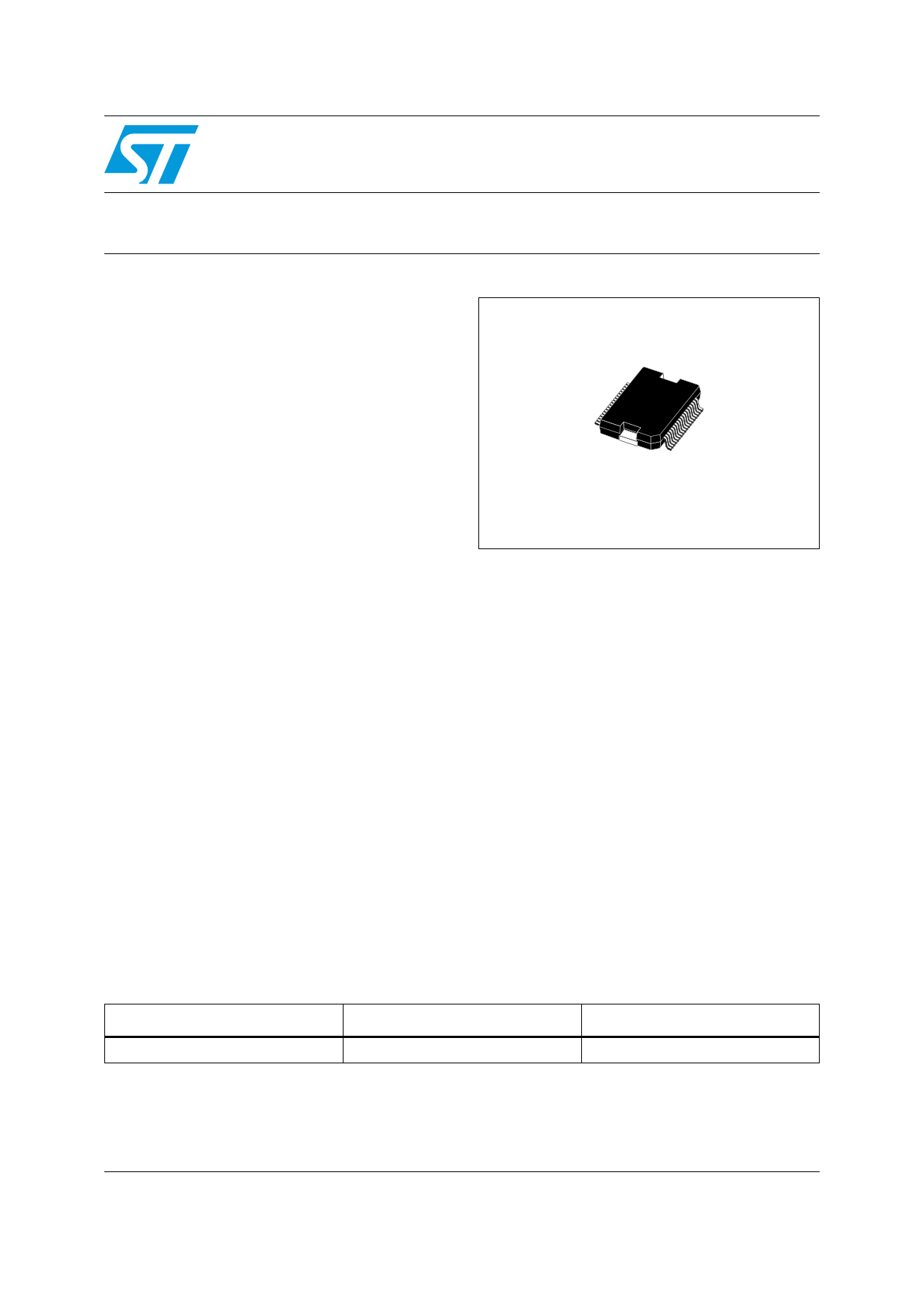
PowerSO36
Protections
■ Over voltage protection
■ Internal current limiting
■ Thermal shutdown
■ ESD
Description
The L5953 is the integration of one switching
regulator, two linear voltage regulators, two low
voltage warnings and two high side drivers. It has
a stand-by operation mode (low current
consumption) where only the stand-by voltage
regulator plus the low voltage warnings are active.
The other regulators and high side drivers are
controlled by the SPI interface.
Table 1.
Device summary
Part number
L5953
Package
PowerSO36
Packing
Tray
September 2007
Rev 2
1/31
www.st.com
1
Free Datasheet http://www.datasheet4u.com/
1 page 
L5953
List of figures
List of figures
Figure 1.
Figure 2.
Figure 3.
Figure 4.
Figure 5.
Figure 6.
Figure 7.
Figure 8.
Figure 9.
Figure 10.
Figure 11.
Figure 12.
Figure 13.
Figure 14.
Figure 15.
Figure 16.
Figure 17.
Figure 18.
Figure 19.
Figure 20.
Figure 21.
Figure 22.
Block diagram . . . . . . . . . . . . . . . . . . . . . . . . . . . . . . . . . . . . . . . . . . . . . . . . . . . . . . . . . . . . 6
PIN connections . . . . . . . . . . . . . . . . . . . . . . . . . . . . . . . . . . . . . . . . . . . . . . . . . . . . . . . . . . 7
AC testing input output waveforms . . . . . . . . . . . . . . . . . . . . . . . . . . . . . . . . . . . . . . . . . . 12
SPI clocking scheme . . . . . . . . . . . . . . . . . . . . . . . . . . . . . . . . . . . . . . . . . . . . . . . . . . . . . 13
Output timing . . . . . . . . . . . . . . . . . . . . . . . . . . . . . . . . . . . . . . . . . . . . . . . . . . . . . . . . . . . 13
Serial input timing . . . . . . . . . . . . . . . . . . . . . . . . . . . . . . . . . . . . . . . . . . . . . . . . . . . . . . . . 13
Linear regulators . . . . . . . . . . . . . . . . . . . . . . . . . . . . . . . . . . . . . . . . . . . . . . . . . . . . . . . . 16
Reset . . . . . . . . . . . . . . . . . . . . . . . . . . . . . . . . . . . . . . . . . . . . . . . . . . . . . . . . . . . . . . . . . 16
Low voltage warning block diagram. . . . . . . . . . . . . . . . . . . . . . . . . . . . . . . . . . . . . . . . . . 16
HSD . . . . . . . . . . . . . . . . . . . . . . . . . . . . . . . . . . . . . . . . . . . . . . . . . . . . . . . . . . . . . . . . . . 17
PWM . . . . . . . . . . . . . . . . . . . . . . . . . . . . . . . . . . . . . . . . . . . . . . . . . . . . . . . . . . . . . . . . . 17
SPI & IRQ . . . . . . . . . . . . . . . . . . . . . . . . . . . . . . . . . . . . . . . . . . . . . . . . . . . . . . . . . . . . . 17
Write enable latch sequence . . . . . . . . . . . . . . . . . . . . . . . . . . . . . . . . . . . . . . . . . . . . . . . 22
Test mode diagnostic procedure start (after a write enable latch sequence. . . . . . . . . . . . 22
Read the diagnostic registerCase1: after a test mode diagnostic procedure start . . . . . . . 22
Diagnostic procedure start (after write enable latch sequence operation A) . . . . . . . . . . . 23
Read the diagnostic RegisterCase2: after a diagnostic procedure start. . . . . . . . . . . . . . . 23
Write the status register (after a write enable latch sequence operation A) . . . . . . . . . . . . 23
Read the status register . . . . . . . . . . . . . . . . . . . . . . . . . . . . . . . . . . . . . . . . . . . . . . . . . . . 23
Block and application diagram . . . . . . . . . . . . . . . . . . . . . . . . . . . . . . . . . . . . . . . . . . . . . . 25
Block diagram and application with external Power MOS . . . . . . . . . . . . . . . . . . . . . . . . . 25
PowerSO36 mechanical data and package dimensions . . . . . . . . . . . . . . . . . . . . . . . . . . 29
5/31
Free Datasheet http://www.datasheet4u.com/
5 Page 
L5953
Block diagram and electrical specifications
Table 5. Electrical characteristics (continued) (Tamb = 25°C, VDD = 14.4V)
Symbol
Parameter
Test condition
Min. Typ. Max. Unit
IRH
VCTth
VCThy
Reset output leakage
Delay comparator threshold
Delay comparator threshold
hysteresis
VRT = VSTBY
0.5 x
VSTBY
10
180
μA
mV
ICT1
Timing capacitor output source
current
7.5 μA
RCT2
Timing capacitor output pull-down
equivalent resistor
150 Ω
Table 6. Diagnostic parameters
Symbol
Parameter
HSD1W1
High side driver 1 overcurrent
warning activation
HSD1W2
High side driver 1 open load
warning activation
HSD1W2 High side driver 1 vdd short
TEST warning activation in test mode
HSD2W1
HSD2W2
High side driver 2 overcurrent
warning activation
High side driver 2 open load
warning activation
HSD2W3
High side driver 2 vdd short
warning activation in test mode
THW Thermal warning activation
IRQ - Interrupt request pin
IRQ-L
IRQ-H
IRQ low voltage
IRQ leakage
Test condition
Min. Typ. Max. Unit
1A
HSD1 output voltage in test mode
3
HSD1 in test mode
measure VVDD-LIN-VHSD1
1 1.5 2
0.5
V
V
A
HSD2 output voltage in test mode
3
HSD2 in test mode
measure VVDD-LIN-VHSD1
1 1.5 2
145
V
V
°C
Io = 1mA
Virq = 5V
0.4 V
1 μA
Table 7. SPI interface
Symbol
Alt
Parameter
Test conditions
Min. Max. Unit
Recommended DC operating voltage
VSPI
Supply voltage for SPI I/O
Input parameters (Tamb = 25°C, f = 1MHz)
CIN Input capacitance (D)
CIN Input capacitance (others pins)
tLPF Input signal pulse width
3 5.5 V
8 pF
6 pF
10 ns
11/31
Free Datasheet http://www.datasheet4u.com/
11 Page | ||
| Páginas | Total 30 Páginas | |
| PDF Descargar | [ Datasheet L5953.PDF ] | |
Hoja de datos destacado
| Número de pieza | Descripción | Fabricantes |
| L5950 | MULTIPLE MULTIFUNCTION VOLTAGE REGULATOR FOR CAR RADIO | STMicroelectronics |
| L5951 | TRIPLE OUTPUT MULTIFUNCTION VOLTAGE REGULATOR FOR CAR RADIO WITH IDR/CLASS 2 INTERFACE | STMicroelectronics |
| L5952 | MULTIPLE MULTIFUNCTION VOLTAGE REGULATOR | STMicroelectronics |
| L5953 | Multiple switching voltage regulator | STMicroelectronics |
| Número de pieza | Descripción | Fabricantes |
| SLA6805M | High Voltage 3 phase Motor Driver IC. |
Sanken |
| SDC1742 | 12- and 14-Bit Hybrid Synchro / Resolver-to-Digital Converters. |
Analog Devices |
|
DataSheet.es es una pagina web que funciona como un repositorio de manuales o hoja de datos de muchos de los productos más populares, |
| DataSheet.es | 2020 | Privacy Policy | Contacto | Buscar |