|
|
PDF CW24C16 Data sheet ( Hoja de datos )
| Número de pieza | CW24C16 | |
| Descripción | (CW24C02 - CW24C16) I2C Bus EEPROM | |
| Fabricantes | ChipsWinner | |
| Logotipo |  |
|
Hay una vista previa y un enlace de descarga de CW24C16 (archivo pdf) en la parte inferior de esta página. Total 17 Páginas | ||
|
No Preview Available !
CW24C02/ CW24C04/ CW24C08/ CW24C16
2Kbit, 4Kbit, 8Kbit and 16Kbit Serial I²C Bus EEPROM
DESCRIPTION
PIN CONFIGURATION
The CW24C02/04/08/16 is Electrically Erasable PROM. The
device is organized as one block of 256/512/1024/2048 x 8-bit
memory with 2-wire serial interface. Low-voltage design permits
operation down to 1.8V, with standby and active currents of only
1μA and 1mA respectively. The CW24C02/04/08/16 also has a
page write capability for up to 8/16/16/16 bytes of data.
A0
A1
A2
GND
18
27
C02
36
45
VCC
WP
SCL
SDA
NC 1
8 VCC
FEATURES
● Wide Voltage Operation VCC= 1.8V to 5.5V
● Low-power technology
A1
A2
GND
27
C04
36
45
WP
SCL
SDA
- 1mA Active Current Typical
- 1μA Standby Current Typical
● Internally Organized:
- CW24C02, 256 X 8 (2K bits)
- CW24C04, 512 X 8 (4K bits)
- CW24C08, 1024 X 8 (8K bits)
NC
NC
A2
GND
18
27
C08
36
45
VCC
WP
SCL
SDA
- CW24C16, 2048 X 8 (16K bits)
● Two-wire Serial Interface, Fully I2C Bus Compatible
● 1 MHz (5V), 400 kHz (1.8V, 2.5V, 2.7V) Compatibility
● Schmitt Trigger Inputs for Noise Suppression
● Write Protect Pin for Hardware Data Protection
● Self-timed Write Cycle (5 ms max)
NC
NC
NC
GND
18
27
3 C16 6
45
VCC
WP
SCL
SDA
● Byte and Multi-byte Write
● Page Write, 8-byte Page (CW24C02), 16-byte Page (CW24C04/08/16) (Top View)
● Byte, Random and Sequential Read Mode
● Automatic Address Incrementing
● ESD protection > 2.5KV
● High-reliability
- Endurance: 1 Million Write Cycles
- Data Retention: 100 Years
● DIP8L, SOP8L,TSSOP8 and DFN8 Packages
● Pb-free finish available, RoHS compliant
APPLICATIONS
● Intelligent Instrument
● Industrial Controller
● Household Appliance
● Automotive Electronics
● Computer/Notebook
● Communication
September. 2007
Rev 1.1
1
Free Datasheet http://www.datasheet4u.com/
1 page 
CW24C02/ CW24C04/ CW24C08/ CW24C16
AC ELECTRICAL CHARACTERISTICS(CONTINUED)
Parameter
Symbol Test Conditions
Min Typ
Start Hold Time
tHD.STA
VCC =1.8V
VCC =5V
0.6
0.25
Start Setup Time
Data In Hold Time
tSU.STA
tHD.DAT
VCC =1.8V
VCC =5V
0.6
0.25
0
Data In Setup Time
tSU.DAT
100
Inputs Rise Time
Inputs Fall Time
tR
VCC =1.8V
tF
VCC =5V
Stop Setup Time
tSU.STO
VCC =1.8V
VCC =5V
0.6
0.25
Data Out Hold Time
tDH
50
Write Cycle Time
tWR
Max Unit
μs
μs
μs
ns
300 ns
300
ns
100
μs
ns
5 ms
SCL
tSU.STA
tF
tLOW
tHD.STA
tHIGH
tLOW
tHD.DAT
tSU.DAT
tR
tSU.STO
SDA_IN
tAA tDH
tBUF
SDA_OUT
Figure 2. Bus Timing
SCL
SDA
8th BIT
ACK
tW
(1)
R
STOP
CONDITION
START
CONDITION
NOTE 1. The write cycle time tWR is the time from a valid stop condition of a write
sequence to the end of the internal clear/write cycle.
Figure 3. Write Cycle Timing
September. 2007
Rev 1.1
5
5 Page 
CW24C02/ CW24C04/ CW24C08/ CW24C16
DETAILED OPERATING INFORMATION(CONTINUED)
SW
TR
AI
R DEVICE T
T ADDRESS E
WORD
ADDRESS(n)
DATA( n )
DATA( n+1 )
DATA( n+x )
S
T
O
P
SDA LINE
M L R AM
LA
A
A
A
S S / CS
SC
C
C
C
B BWKB
BK
K
K
K
Figure 10. Page Write
3. Acknowledge Polling
Once the internally timed write cycle has started and the EEPROM inputs are disabled, acknowl-
edge polling can be initiated. This involves sending a start condition followed by the device
address word. The read/write bit is representative of the operation desired. Only if the internal
write cycle has completed will the EEPROM respond with a "0", allowing the read or write
sequence to continue. See Figure 11 for flow diagram
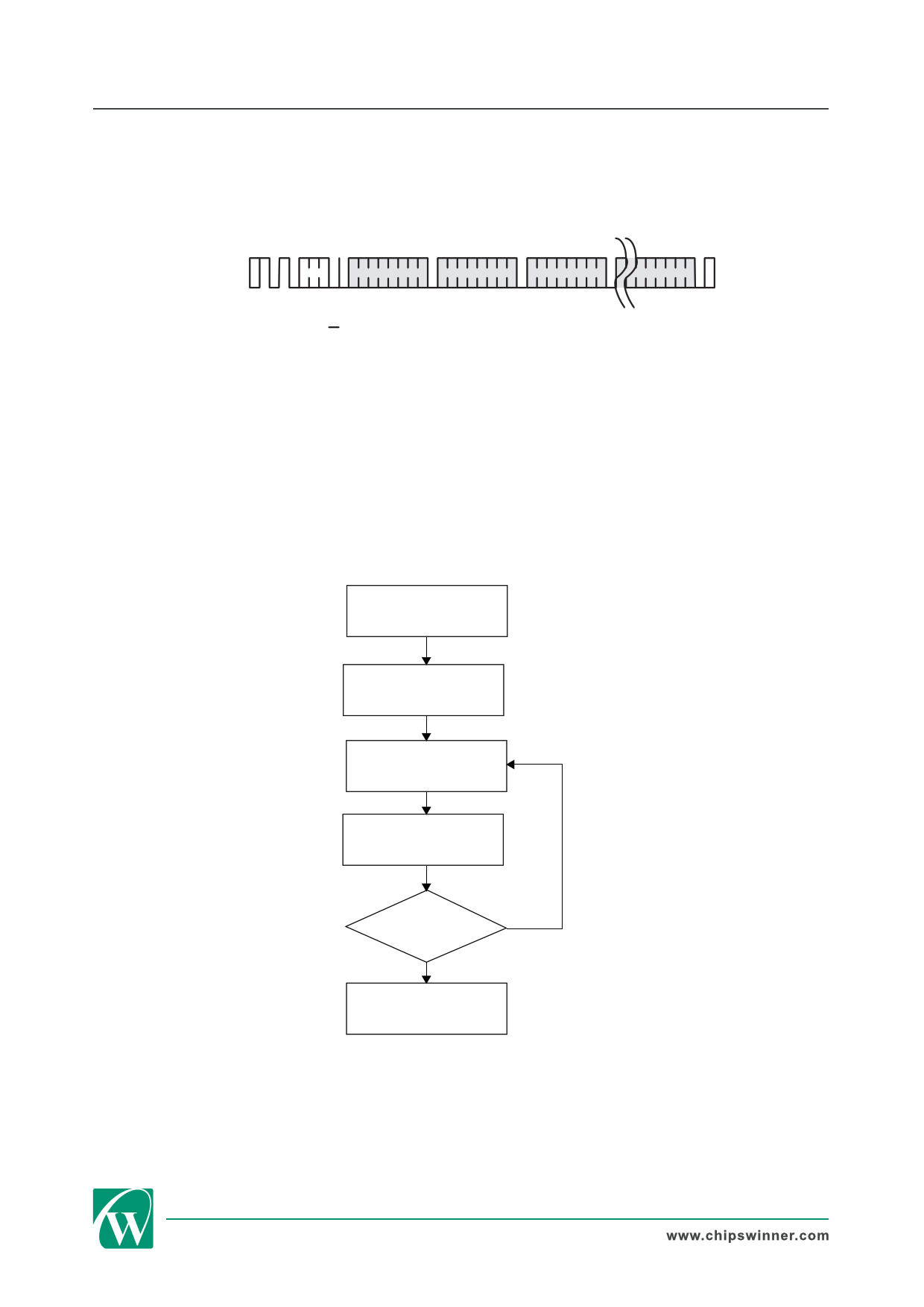
Send
Write Command
Send Stop
Condition to
Initiate Write Cycle
Send Start
Send Control Byte
with R/W = 0
Did Device
Acknowledge
(ACK = 0)?
YES
Next
Operation
NO
Figure 11. Acknowdge Polling Flow
Read Operations
Read operations are initiated the same way as write operations with the exception that the
read/write select bit in the device address word is set to "1". There are three read operations:
current address read, random address read and sequential read.
September. 2007
Rev 1.1
11
11 Page | ||
| Páginas | Total 17 Páginas | |
| PDF Descargar | [ Datasheet CW24C16.PDF ] | |
Hoja de datos destacado
| Número de pieza | Descripción | Fabricantes |
| CW24C128 | 128Kbit and 256Kbit Serial I2C Bus EEPROM | ChipsWinner |
| CW24C16 | (CW24C02 - CW24C16) I2C Bus EEPROM | ChipsWinner |
| Número de pieza | Descripción | Fabricantes |
| SLA6805M | High Voltage 3 phase Motor Driver IC. |
Sanken |
| SDC1742 | 12- and 14-Bit Hybrid Synchro / Resolver-to-Digital Converters. |
Analog Devices |
|
DataSheet.es es una pagina web que funciona como un repositorio de manuales o hoja de datos de muchos de los productos más populares, |
| DataSheet.es | 2020 | Privacy Policy | Contacto | Buscar |
