|
|
|
PDF K210 Data sheet ( Hoja de datos )
| Número de pieza | K210 | |
| Descripción | MOSFET ( Transistor ) - 2SK210 | |
| Fabricantes | Toshiba Semiconductor | |
| Logotipo | ||
Hay una vista previa y un enlace de descarga de K210 (archivo pdf) en la parte inferior de esta página. Total 6 Páginas | ||
|
No Preview Available !
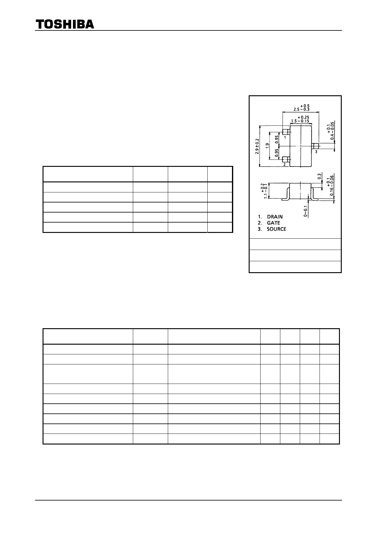
TOSHIBA Field Effect Transistor Silicon N Channel Junction Type
2SK210
FM Tuner Applications
VHF Band Amplifier Applications
2SK210
Unit: mm
• High power gain: GPS = 24dB (typ.) (f = 100 MHz)
• Low noise figure: NF = 1.8dB (typ.) (f = 100 MHz)
• High forward transfer admittance: |Yfs| = 7 mS (typ.) (f = 1 kHz)
Absolute Maximum Ratings (Ta = 25°C)
Characteristics
Symbol
Rating
Unit
Gate-drain voltage
Gate current
Drain power dissipation
Junction temperature
Storage temperature range
VGDO
IG
PD
Tj
Tstg
−18
10
100
125
−55~125
V
mA
mW
°C
°C
Note: Using continuously under heavy loads (e.g. the application of high
temperature/current/voltage and the significant change in
JEDEC
―
temperature, etc.) may cause this product to decrease in the
JEITA
SC-59
reliability significantly even if the operating conditions (i.e.
operating temperature/current/voltage, etc.) are within the
TOSHIBA
2-3F1C
absolute maximum ratings.
http://www.DataSheet4U.net/
Weight: 0.012 g (typ.)
Please design the appropriate reliability upon reviewing the
Toshiba Semiconductor Reliability Handbook (“Handling Precautions”/“Derating Concept and Methods”) and
individual reliability data (i.e. reliability test report and estimated failure rate, etc).
Electrical Characteristics (Ta = 25°C)
Characteristics
Symbol
Test Condition
Min Typ. Max Unit
Gate leakage current
Gate-drain breakdown voltage
Drain current
Gate-source cut-off voltage
Forward transfer admittance
Input capacitance
Reverse transfer capacitance
Power gain
Noise figure
IGSS
VGS = −1.0 V, VDS = 0 V
V (BR) GDO IG = −100 μA
IDSS
(Note)
VGS = 0 V, VDS = 10 V
VGS (OFF) VDS = 10 V, ID = 1 μA
⎪Yfs⎪
VGS = 0 V, VDS = 10 V, f = 1 kHz
Ciss VDS = 10 V, VGS = 0, f = 1 MHz
Crss
GPS
NF
VGD = −10 V, f = 1 MHz
VDD = 10 V, f = 100 MHz (Figure 1)
VDD = 10 V, f = 100 MHz (Figure 1)
⎯ ⎯ −10 nA
−18 ⎯
⎯
V
3 ⎯ 24 mA
−1.2 −3
⎯
V
⎯ 7 ⎯ mS
⎯ 3.5 ⎯ pF
⎯ ⎯ 0.65 pF
⎯ 24 ⎯ dB
⎯ 1.8 3.5 dB
Note: IDSS classificatopn Y: 3.0~7.0 mA, GR (R): 6.0~14.0 mA, BL (L): 12.0~24.0 mA
1 2007-11-01
datasheet pdf - http://www.DataSheet4U.net/
1 page 
2SK210
http://www
5 2007-11-01
da
5 Page | ||
| Páginas | Total 6 Páginas | |
| PDF Descargar | [ Datasheet K210.PDF ] | |
Hoja de datos destacado
| Número de pieza | Descripción | Fabricantes |
| K210 | LOW LEVEL ZENER DIODES VERY LOW VOLTAGE/ LOW LEAKAGE | Knox Semiconductor |
| K210 | LOW LEVEL ZENER DIODES VERY LOW VOLTAGE/ LOW LEAKAGE | Knox Inc |
| K210 | MOSFET ( Transistor ) - 2SK210 | Toshiba Semiconductor |
| K2101 | MOSFET ( Transistor ) - 2SK2101 | Fuji Electric |
| Número de pieza | Descripción | Fabricantes |
| SLA6805M | High Voltage 3 phase Motor Driver IC. |
Sanken |
| SDC1742 | 12- and 14-Bit Hybrid Synchro / Resolver-to-Digital Converters. |
Analog Devices |
|
DataSheet.es es una pagina web que funciona como un repositorio de manuales o hoja de datos de muchos de los productos más populares, |
| DataSheet.es | 2020 | Privacy Policy | Contacto | Buscar |