|
|
|
PDF FOD8320 Data sheet ( Hoja de datos )
| Número de pieza | FOD8320 | |
| Descripción | Logic Output Photocouplers | |
| Fabricantes | Fairchild Semiconductor | |
| Logotipo | ||
Hay una vista previa y un enlace de descarga de FOD8320 (archivo pdf) en la parte inferior de esta página. Total 18 Páginas | ||
|
No Preview Available !
March 2012
FOD8320
High Noise Immunity, 2.5A Output Current, Gate Drive
Optocoupler in Optoplanar® Wide Body SOP 5-Pin
Features
■ Fairchild’s Optoplanar® packaging technology
provides reliable and high voltage insulation with
greater than 10mm creepage and clearance distance,
and 0.5mm internal insulation distance while still
offering a compact footprint
■ 2.5A output current driving capability for medium
power IGBT/MOSFET
– Use of P-Channel MOSFETs at output stage
enables output voltage swing close to the supply
rail
■ 35kV/µs Minimum Common Mode Rejection
■ Wide Supply Voltage range from 15V to 30V
■ Fast Switching Speed over full operating temperature
range
– 400ns max. propagation delay
– 100ns max. pulse width distortion
■ UnderVoltage LockOut (UVLO) with hysteresis
■ Extended industrial temperate range, -40 to 100°C
temperature range
■ Safety and regulatory approvals
– UL1577, 5,000VRMS for 1 min.
– DIN EN/IEC60747-5-2 (pending approval)
Applications
■ AC and brushless DC motor drives
■ Industrial inverter
■ Uninterruptible power supply
■ Induction heating
■ Isolated IGBT/Power MOSFET gate drive
Related Resources
■ FOD3120, High Noise Immunity, 2.5A Output Current,
Gate Drive Optocoupler Datasheet
Description
The FOD8320 is a 2.5A Output Current Gate Drive
Optocoupler, capable of driving medium power IGBT/
MOSFETs. It is ideally suited for fast switching driving of
power IGBT and MOSFETs used in motor control
inverter applications, and high performance power
systems.
It utilizes Fairchild’s coplanar packaging technology,
Optoplanar®, and optimized IC design to achieve reliably
high insulation voltage and high noise immunity.
It consists of a aluminum gallium arsenide (AlGaAs) light
emitting diode optically coupled to an integrated circuit
with a high-speed driver for push-pull MOSFET output
stage. The device is housed in a wide body 5-pin small
outline plastic package.
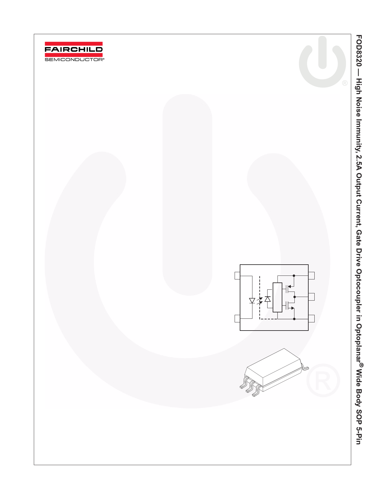
Functional Schematic
ANODE 1
CATHODE 3
6 VDD
5 VO
4 VSS
©2010 Fairchild Semiconductor Corporation
FOD8320 Rev. 1.0.4
www.fairchildsemi.com
1 page 
Isolation Characteristics
Apply over all recommended conditions, typical value is measured at TA = 25ºC
Symbol
Parameter
Conditions
Min. Typ. Max. Units
VISO
RISO
CISO
Input-Output Isolation
Voltage
Isolation Resistance
Isolation Capacitance
TA = 25ºC, R.H. < 50%, t = 1.0min,
II-O ≤ 20µA, 50Hz(5)(6)
VI-O = 500V(5)
VI-O = 0V, Freq = 1.0MHz(6)
5,000
1011
1
VRMS
Ω
pF
Notes:
5. Device is considered a two terminal device: Pins 1 and 3 are shorted together and Pins 4, 5 and 6 are shorted
together.
6. 5,000 VACRMS for 1 minute duration is equivalent to 6,000 VACRMS for 1 second duration.
Electrical Characteristics
Apply over all recommended conditions, typical value is measured at VDD = 30V, VSS = Ground, TA = 25°C unless
otherwise specified.
Symbol
Parameter
Conditions
Min.
Typ.
Max. Units Figure
VF
∆(VF / TA)
BVR
CIN
IOH
IOL
VOH
VOL
IDDH
IDDL
IFLH
VFHL
VUVLO+
VUVLO-
UVLOHYS
Input Forward Voltage
IF = 10mA
Temperature Coefficient of
Forward Voltage
Input Reverse Breakdown IR = 10µA
Voltage
Input Capacitance
f = 1MHz, VF = 0V
High Level Output
Current(7)
VOH = VDD – 3V
VOH = VDD – 6V
Low Level Output
Current(7)
VOL = VSS + 3V
VOL = VSS+ 6V
High Level Output
Voltage(7)(8)
IF = 10mA, IO = -2.5A
IF = 10mA, IO = -100mA
Low Level Output
Voltage(7)(8)
IF = 10mA, IO = 2.5A
IF = 0mA, IO = 100mA
High Level Supply Current VO Open, IF = 7 to 16mA
Low Level Supply Current VO Open, VF = 0 to 0.8V
Threshold Input Current
Low to High
IO = 0mA, VO > 5V
Threshold Input Voltage
High to Low
IO = 0mA, VO < 5V
UnderVoltage Lockout
Threshold
UnderVoltage Lockout
Threshold Hysteresis
IF = 10mA, VO > 5V
IF = 10mA, VO < 5V
1.1 1.5 1.8 V 16
-1.8 mV/°C
5V
60 pF
1.0 2.0 2.5 A 1, 3
2.0 2.5 A 1, 3, 19
1.0 2.0 2.5 A 4, 6
2.0 2.5 A 4, 6, 18
VDD – 6.25
VDD – 0.5
VDD – 2.5
VDD – 0.1
VSS + 2.5
VSS + 0.1
2.9
VSS + 6.25
VSS + 0.5
3.8
V
V
mA
1
1, 2, 20
4
5, 21
7, 8, 22
2.8 3.8 mA 7, 8, 23
2.4 5.0 mA 9, 15, 24
0.8 V 25
11.5 12.7 14.5 V 17, 26
10.0 11.2 13.0 V 17, 26
1.5 V
Notes:
7. In this test, VOH is measured with a dc load current of 100mA. When driving capacitive load VOH will approach VDD
as IOH approaches zero amps.
8. Maximum pulse width = 1ms, maximum duty cycle = 20%.
©2010 Fairchild Semiconductor Corporation
FOD8320 Rev. 1.0.4
5
www.fairchildsemi.com
5 Page 
Test Circuit (Continued)
1
IF = 7 to 16mA
3
6
0.1µF
5
VO
+
–
VDD = 15 to 30V
100mA
4
Figure 20. VOH Test Circuit
16
0.1µF
5
100mA
VO
+
–
VDD = 15 to 30V
34
Figure 21. VOL Test Circuit
©2010 Fairchild Semiconductor Corporation
FOD8320 Rev. 1.0.4
11
www.fairchildsemi.com
11 Page | ||
| Páginas | Total 18 Páginas | |
| PDF Descargar | [ Datasheet FOD8320.PDF ] | |
Hoja de datos destacado
| Número de pieza | Descripción | Fabricantes |
| FOD8320 | Logic Output Photocouplers | Fairchild Semiconductor |
| FOD8321 | Gate Drive Optocoupler | Fairchild Semiconductor |
| Número de pieza | Descripción | Fabricantes |
| SLA6805M | High Voltage 3 phase Motor Driver IC. |
Sanken |
| SDC1742 | 12- and 14-Bit Hybrid Synchro / Resolver-to-Digital Converters. |
Analog Devices |
|
DataSheet.es es una pagina web que funciona como un repositorio de manuales o hoja de datos de muchos de los productos más populares, |
| DataSheet.es | 2020 | Privacy Policy | Contacto | Buscar |