|
|
|
PDF CY14E512Q Data sheet ( Hoja de datos )
| Número de pieza | CY14E512Q | |
| Descripción | 512-Kbit (64 K x 8) SPI nvSRAM | |
| Fabricantes | Cypress Semiconductor | |
| Logotipo | ||
Hay una vista previa y un enlace de descarga de CY14E512Q (archivo pdf) en la parte inferior de esta página. Total 30 Páginas | ||
|
No Preview Available !
CY14C512Q
CY14B512Q
CY14E512Q
512-Kbit (64 K × 8) SPI nvSRAM
512-Kbit (64 K × 8) SPI nvSRAM
Features
■ 512-Kbit nonvolatile static random access memory (nvSRAM)
internally organized as 64 K × 8
❐ STORE to QuantumTrap nonvolatile elements initiated
automatically on power-down (AutoStore) or by using SPI
instruction (Software STORE) or HSB pin (Hardware
STORE)
❐ RECALL to SRAM initiated on power-up (Power-Up
RECALL) or by SPI instruction (Software RECALL)
❐ Support automatic STORE on power-down with a small
capacitor (except for CY14X512Q1A)
■ High reliability
❐ Infinite read, write, and RECALL cycles
❐ 1million STORE cycles to QuantumTrap
❐ Data retention: 20 years at 85 C
■ 40-MHz, and 104-MHz High-speed serial peripheral interface
(SPI)
❐ 40-MHz clock rate SPI write and read with zero cycle delay
❐ 104-MHz clock rate SPI write and SPI read (with special fast
read instructions)
❐ Supports SPI mode 0 (0,0) and mode 3 (1,1)
■ SPI access to special functions
❐ Nonvolatile STORE/RECALL
❐ 8-byte serial number
❐ Manufacturer ID and Product ID
❐ Sleep mode
■ Write protection
❐ Hardware protection using Write Protect (WP) pin
❐ Software protection using Write Disable instruction
❐ Software block protection for 1/4, 1/2, or entire array
■ Low power consumption
❐ Average active current of 3 mA at 40 MHz operation
❐ Average standby mode current of 150 A
❐ Sleep mode current of 8 A
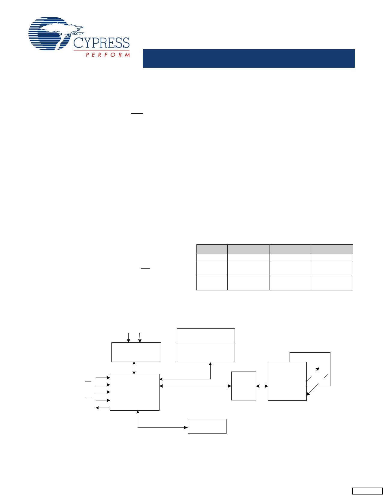
Logic Block Diagram
VCC VCAP
■ Industry standard configurations
❐ Operating voltages:
• CY14C512Q: VCC = 2.4 V to 2.6 V
• CY14B512Q: VCC = 2.7 V to 3.6 V
• CY14E512Q: VCC = 4.5 V to 5.5 V
❐ Industrial temperature
❐ 8- and 16-pin small outline integrated circuit (SOIC) package
❐ Restriction of hazardous substances (RoHS) compliant
Functional Overview
The Cypress CY14X512Q combines a 512-Kbit nvSRAM[1] with
a nonvolatile element in each memory cell with serial SPI
interface. The memory is organized as 64 K words of 8 bits each.
The embedded nonvolatile elements incorporate the
QuantumTrap technology, creating the world’s most reliable
nonvolatile memory. The SRAM provides infinite read and write
cycles, while the QuantumTrap cells provide highly reliable
nonvolatile storage of data. Data transfers from SRAM to the
nonvolatile elements (STORE operation) takes place
automatically at power-down (except for CY14X512Q1A). On
power-up, data is restored to the SRAM from the nonvolatile
memory (RECALL operation). You can also initiate the STORE
and RECALL operations through SPI instruction.
Configuration
Feature
AutoStore
Software
STORE
Hardware
STORE
CY14X512Q1A
No
Yes
CY14X512Q2A
Yes
Yes
CY14X512Q3A
Yes
Yes
No No Yes
Serial Number
8x8
SI
CS
SCK
WP
SO
Power Control
Block
SLEEP
SPI Control Logic
Write Protection
Instruction decoder
Manufacture ID/
Product ID
RDSN/WRSN/RDID
READ/WRITE
STORE/RECALL/ASENB/ASDISB
Memory
Data &
Address
Control
QuantrumTrap
64 K x 8
SRAM
64 K x 8
STORE
RECALL
WRSR/RDSR/WREN
Status Register
Note
1. This device will be referred to as nvSRAM throughout the document.
Cypress Semiconductor Corporation • 198 Champion Court
wwwD.DocautamSheenett4#U: .0n0et1-65267 Rev. *B
• San Jose, CA 95134-1709 • 408-943-2600
Revised May 5, 2011
[+] Feedback
1 page 
CY14C512Q
CY14B512Q
CY14E512Q
previous nonvolatile data is first performed, followed by a
program of the nonvolatile elements. After a STORE cycle is
initiated, read/write to CY14X512Q is inhibited until the cycle is
completed.
The HSB signal or the RDY bit in the Status Register can be
monitored by the system to detect if a STORE or Software
RECALL cycle is in progress. The busy status of nvSRAM is
indicated by HSB being pulled LOW or RDY bit being set to ‘1’.
To avoid unnecessary nonvolatile STOREs, AutoStore and
Hardware STORE operations are ignored unless at least one
write operation has taken place since the most recent STORE or
RECALL cycle. However, software initiated STORE cycles are
performed regardless of whether a write operation has taken
place.
AutoStore Operation
The AutoStore operation is a unique feature of nvSRAM which
automatically stores the SRAM data to QuantumTrap cells
during power-down. This STORE makes use of an external
capacitor (VCAP) and enables the device to safely STORE the
data in the nonvolatile memory when power goes down.
During normal operation, the device draws current from VCC to
charge the capacitor connected to the VCAP pin. When the
voltage on the VCC pin drops below VSWITCH during power-down,
the device inhibits all memory accesses to nvSRAM and
automatically performs a conditional STORE operation using the
charge from the VCAP capacitor. The AutoStore operation is not
initiated if no write cycle has been performed since last RECALL.
Note If a capacitor is not connected to VCAP pin, AutoStore must
be disabled by issuing the AutoStore Disable instruction
(AutoStore Disable (ASDISB) Instruction on page 15). If
AutoStore is enabled without a capacitor on the VCAP pin, the
device attempts an AutoStore operation without sufficient charge
to complete the STORE. This will corrupt the data stored in
nvSRAM, Status Register as well as the serial number and it will
unlock the SNL bit. To resume normal functionality, the WRSR
instruction must be issued to update the nonvolatile bits BP0,
BP1, and WPEN in the Status Register.
Figure 3 shows the proper connection of the storage capacitor
(VCAP) for AutoStore operation. Refer to DC Electrical
Characteristics on page 21 for the size of the VCAP.
Note CY14X512Q1A does not support AutoStore operation. You
must perform Software STORE operation by using the SPI
STORE instruction to secure the data.
Figure 3. AutoStore Mode
VCC
0.1 uF
VCC
Software STORE Operation
Software STORE enables the user to trigger a STORE operation
through a special SPI instruction. STORE operation is initiated
by executing STORE instruction irrespective of whether a write
has been performed since the last NV operation.
A STORE cycle takes tSTORE time to complete, during which all
the memory accesses to nvSRAM are inhibited. The RDY bit of
the Status Register or the HSB pin may be polled to find the
Ready or Busy status of the nvSRAM. After the tSTORE cycle time
is completed, the SRAM is activated again for read and write
operations.
Hardware STORE and HSB pin Operation
The HSB pin in CY14X512Q3A is used to control and
acknowledge STORE operations. If no STORE or RECALL is in
progress, this pin can be used to request a Hardware STORE
cycle. When the HSB pin is driven LOW, nvSRAM conditionally
initiates a STORE operation after tDELAY duration. A STORE
cycle starts only if a write to the SRAM has been performed since
the last STORE or RECALL cycle. Reads and Writes to the
memory are inhibited for tSTORE duration or as long as HSB pin
is LOW. The HSB pin also acts as an open drain driver (internal
100 k weak pull up resistor) that is internally driven LOW to
indicate a busy condition when the STORE (initiated by any
means) is in progress.
Note After each Hardware and Software STORE operation HSB
is driven HIGH for a short time (tHHHD) with standard output high
current and then remains HIGH by an internal 100 k pull up
resistor.
Note For successful last data byte STORE, a hardware STORE
should be initiated at least one clock cycle after the last data bit
D0 is received.
Upon completion of the STORE operation, the nvSRAM memory
access is inhibited for tLZHSB time after HSB pin returns HIGH.
The HSB pin must be left unconnected if not used.
Note CY14X512Q1A/CY14X512Q2A do not have HSB pin. RDY
bit of the SPI Status Register may be probed to determine the
Ready or Busy status of nvSRAM.
RECALL Operation
A RECALL operation transfers the data stored in the nonvolatile
QuantumTrap elements to the SRAM. A RECALL may be
initiated in two ways: Hardware RECALL, initiated on power-up
and Software RECALL, initiated by a SPI RECALL instruction.
Internally, RECALL is a two step procedure. First, the SRAM data
is cleared. Next, the nonvolatile information is transferred into the
SRAM cells. All memory accesses are inhibited while a RECALL
cycle is in progress. The RECALL operation does not alter the
data in the nonvolatile elements.
CS VCAP
VSS
VCAP
Document #: 001-65267 Rev. *B
Page 5 of 33
[+] Feedback
5 Page 
CY14C512Q
CY14B512Q
CY14E512Q
Figure 7. Read Status Register (RDSR) Instruction Timing
CS
SCK
SI
0 1 2 3 4 5 67 01 2 3 4 5 67
Op-Code
0 0 0 0 01 0 1 0
CS
SCK
SI
SO HI-Z D7 D6 D5 D4 D3 D2 D1 D0
MSB
Data
LSB
Figure 8. Fast Read Status Register (FAST_RDSR) Instruction Timing
0 1 2 3 4 5 6 7 8 9 10 11 12 13 14 15 0 1 2 3 4 5 6 7
Op-Code
Dummy Byte
0 0 0 0 1 00 1 XXXXX XXX 0
SO
HI-Z
D7 D6 D5 D4 D3 D2 D1 D0
MSB
Data
LSB
Figure 9. Write Status Register (WRSR) Instruction Timing
CS
SCK
01 23 4 5 6 701 2 3 4 5 6 7
Opcode
Data in
SI 0 0 0 0 0 0 0 1 D7 X X X D3 D2 X X
MSB
LSB
SO HI-Z
Write Protection and Block Protection
CY14X512Q provides features for both software and hardware
write protection using WRDI instruction and WP. Additionally, this
device also provides block protection mechanism through BP0
and BP1 pins of the Status Register.
The write enable and disable status of the device is indicated by
WEN bit of the Status Register. The write instructions (WRSR
WRITE and WRSN) and nvSRAM special instruction (STORE,
RECALL, ASENB and ASDISB) need the write to be enabled
(WEN bit = ‘1’) before they can be issued.
must therefore be preceded by a Write Enable instruction. If the
device is not write enabled (WEN = ‘0’), it ignores the write
instructions and returns to the standby state when CS is brought
HIGH. A new CS falling edge is required to re-initiate serial
communication. The instruction is issued following the falling
edge of CS. When this instruction is used, the WEN bit of Status
Register is set to ‘1’. WEN bit defaults to ‘0’ on power-up.
Note After completion of a write instruction (WRSR, WRITE and
WRSN) or nvSRAM special instruction (STORE, RECALL,
ASENB, and ASDISB) instruction, WEN bit is cleared to ‘0’. This
is done to provide protection from any inadvertent writes.
Write Enable (WREN) Instruction
On power-up, the device is always in the write disable state. The
following WRITE, WRSR, WRSN, or nvSRAM special instruction
Document #: 001-65267 Rev. *B
Page 11 of 33
[+] Feedback
11 Page | ||
| Páginas | Total 30 Páginas | |
| PDF Descargar | [ Datasheet CY14E512Q.PDF ] | |
Hoja de datos destacado
| Número de pieza | Descripción | Fabricantes |
| CY14E512I | 512-Kbit (64 K x 8) Serial (I2C) nvSRAM | Cypress Semiconductor |
| CY14E512J | 512-Kbit (64 K x 8) Serial (I2C) nvSRAM | Cypress Semiconductor |
| CY14E512PA | 512-Kbit (64 K x 8) SPI nvSRAM | Cypress Semiconductor |
| CY14E512Q | 512-Kbit (64 K x 8) SPI nvSRAM | Cypress Semiconductor |
| Número de pieza | Descripción | Fabricantes |
| SLA6805M | High Voltage 3 phase Motor Driver IC. |
Sanken |
| SDC1742 | 12- and 14-Bit Hybrid Synchro / Resolver-to-Digital Converters. |
Analog Devices |
|
DataSheet.es es una pagina web que funciona como un repositorio de manuales o hoja de datos de muchos de los productos más populares, |
| DataSheet.es | 2020 | Privacy Policy | Contacto | Buscar |