|
|
|
PDF LT3652HV Data sheet ( Hoja de datos )
| Número de pieza | LT3652HV | |
| Descripción | Power Tracking 2A Battery Charger | |
| Fabricantes | Linear Technology | |
| Logotipo | ||
Hay una vista previa y un enlace de descarga de LT3652HV (archivo pdf) en la parte inferior de esta página. Total 24 Páginas | ||
|
No Preview Available !
www.DataSheet4U.com
LT3652HV
Power Tracking 2A Battery
Charger
FEATURES
n Input Supply Voltage Regulation Loop for Peak
Power Tracking in (MPPT) Solar Applications
n Wide Input Voltage Range: 4.95V to 34V (40V Abs Max)
n Programmable Charge Rate Up to 2A
n User Selectable Termination: C/10 or On-Board
Termination Timer
n Resistor Programmable Float Voltage Up to 18V
Accommodates 4-Cell Li-Ion/Polymer, 5-Cell
LiFePO4, Lead-Acid Chemistries
n Parallelable for Higher Output Current
n 1MHz Fixed Frequency
n 0.5% Float Voltage Reference Accuracy
n 5% Charge Current Accuracy
n 2.5% C/10 Detection Accuracy
n Binary-Coded Open-Collector Status Pins
APPLICATIONS
n Solar Powered Applications
n Remote Monitoring Stations
n Portable Handheld Instruments
n 12V to 24V Automotive Systems
n Battery Charging from Current Limited Adapter
DESCRIPTION
The LT®3652HV is a complete monolithic step-down bat-
tery charger that operates over a 4.95V to 34V input range.
The LT3652HV provides a constant-current/constant-voltage
charge characteristic, with maximum charge current
externally programmable up to 2A. The charger employs
a 3.3V float voltage feedback reference, so any desired
battery float voltage up to 18V can be programmed with a
resistor divider.
The LT3652HV employs an input voltage regulation loop,
which reduces charge current if the input voltage falls below
a programmed level, set with a resistor divider. When the
LT3652HV is powered by a solar panel, the input regulation
loop is used to maintain the panel at peak output power.
The LT3652HV can be configured to terminate charging when
charge current falls below 1/10 of the programmed maximum
(C/10). Once charging is terminated, the LT3652HV enters a
low-current (85μA) standby mode. An auto-recharge feature
starts a new charging cycle if the battery voltage falls 2.5%
below the programmed float voltage. The LT3652HV also
contains a programmable safety timer, used to terminate
charging after a desired time is reached. This allows top-off
charging at currents less than C/10.
L, LT, LTC, LTM, Linear Technology and the Linear logo are registered trademarks and
PowerPath is a trademark of Linear Technology Corporation. All other trademarks are the
property of their respective owners.
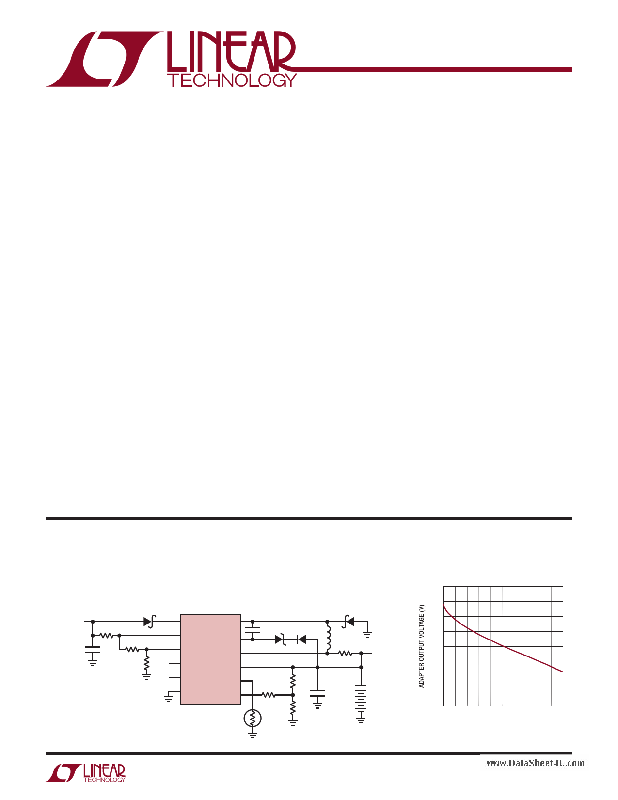
TYPICAL APPLICATION
VIN_REG Loop Servos Maximum Charge Current to Prevent AC Adapter Output from
Drooping Lower Than 24V 5-Cell LiFePO4 Charger (18V at 1.5A) with C/10 Termination
Powered by Inexpensive 24VDC/1A Unregulated Wall Adapter.
AC ADAPTER
INPUT
24VDC AT 1A
MBRS340
750k
10μF
44.2k
51.1k
VIN SW
LT3652HV
VIN_REG
BOOST
SHDN
SENSE
CHRG
BAT
FAULT
NTC
TIMER
VFB
3652 TA01a
1μF 10V 1N4148
D3
MBRS340
20μH
0.068
SYSTEM
LOAD
127k
665k
R1
10K
B = 3380
150k
+
10μF
5-Cell LiFePO4 PACK
(18V FLOAT)
1A/24VDC Unregulated Adapter
I vs V Characteristic
36
33
30
27
24
21
18
15
12
0 0.2 0.4 0.6 0.8 1 1.2 1.4 1.6 1.8 2
ADAPTER OUTPUT CURRENT (A)
3652 TA01b
3652hvf
1
1 page 
www.DataSheet4U.com
LT3652HV
TYPICAL PERFORMANCE CHARACTERISTICS TJ = 25°C, unless otherwise noted.
VIN_REG Threshold
vs Temperature: ICHG at 50%
2.720
2.715
2.710
2.705
2.700
2.695
2.690
2.685
2.680
–50 –25
0 25 50 75
TEMPERATURE (°C)
100 125
3652 G01
VFB Reference Voltage
vs Temperature
3.304
3.302
3.300
3.298
3.296
–50 –25
0 25 50 75
TEMPERATURE (°C)
100 125
3652 G01a
VIN Standby Mode Current
vs Temperature
100
95
90
85
80
75
70
65
–50
–25 0 25 50
TEMPERATURE (°C)
75 100
3652 G02
Switch Drive (ISW/IBOOST)
vs Switch Current
36
33
30
27
24
21
18
15
12
9
6
3
0
0 0.2 0.4 0.6 0.8 1.0 1.2 1.4 1.6 1.8 2.0
SWITCH CURRENT (A)
3652 G03
Switch Forward Drop (VIN – VSW)
vs Temperature
480
ISW = 2A
460
440
420
400
380
360
340
320
–50 –25
0 25 50 75
TEMPERATURE (°C)
100 125
3652 G04
CC/CV Charging; SENSE Pin Bias
Current vs VSENSE
100
VBAT = VBAT(PRE)
50
0
–50 VBAT = VBAT(FLT)
–100
–150
–200
–250
–300
–350
0 0.5 1 1.5 2 2.5
VSENSE (V)
3652 G05
C/10 Threshold (VSENSE–VBAT)
vs Temperature
12
11
10
9
8
–50 –25
0 25 50 75
TEMPERATURE (°C)
100 125
3652 G06
3652hvf
5
5 Page 
www.DataSheet4U.com
LT3652HV
APPLICATIONS INFORMATION
stant-current (CC) mode, which corresponds to 100mV
across RSENSE. The ITH voltage is pulled down to reduce
this maximum charge current should the voltage on the
VIN_REG pin falls below 2.7V (VIN_REG(TH)) or the die tem-
perature approaches 125°C.
If the voltage on the VFB pin is below 2.3V (VFB(PRE)),
the LT3652HV engages precondition mode. During the
precondition interval, the charger continues to operate in
constant-current mode, but the maximum charge current
is reduced to 15% of the maximum programmed value
as set by RSENSE.
When the charger output voltage approaches the float volt-
age, or the voltage on the VFB pin approaches 3.3V (VFB(FLT)),
the charger transitions into constant-voltage (CV) mode
and charge current is reduced from the maximum value.
As this occurs, the ITH voltage falls from the limit clamp
and servos to lower voltages. The IC monitors the ITH volt-
age as it is reduced, and detection of C/10 charge current
is achieved when ITH = 0.1V. If the charger is configured
for C/10 termination, this threshold is used to terminate
the charge cycle. Once the charge cycle is terminated,
the CHRG status pin becomes high-impedance and the
charger enters low-current standby mode.
The LT3652HV contains an internal charge cycle timer that
terminates a successful charge cycle after a programmed
amount of time. This timer is typically programmed to
achieve end-of-cycle (EOC) in 3 hours, but can be con-
figured for any amount of time by setting an appropriate
timing capacitor value (CTIMER). When timer termination
is used, the charge cycle does not terminate when C/10
is achieved. Because the CHRG status pin responds to
the C/10 current level, the IC will indicate a fully-charged
battery status, but the charger continues to source low
currents into the battery until the programmed EOC time
has elapsed, at which time the charge cycle will terminate.
At EOC when the charging cycle terminates, if the battery did
not achieve at least 97.5% of the full float voltage, charging
is deemed unsuccessful, the LT3652HV re-initiates, and
charging continues for another full timer cycle.
Use of the timer function also enables bad-battery detec-
tion. This fault condition is achieved if the battery does
not respond to preconditioning, such that the charger
remains in (or enters) precondition mode after 1/8th of
the programmed charge cycle time. A bad battery fault
halts the charging cycle, the CHRG status pin goes high-
impedance, and the FAULT pin is pulled low.
When the LT3652HV terminates a charging cycle, whether
through C/10 detection or by reaching timer EOC, the
average current mode analog loop remains active, but
the internal float voltage reference is reduced by 2.5%.
Because the voltage on a successfully charged battery is
at the full float voltage, the voltage error amp detects an
over-voltage condition and ITH is pulled low. When the
voltage error amp output drops below 0.3V, the IC enters
standby mode, where most of the internal circuitry is dis-
abled, and the VIN bias current is reduced to 85μA. When
the voltage on the VFB pin drops below the reduced float
reference level, the output of the voltage error amp will
climb, at which point the IC comes out of standby mode
and a new charging cycle is initiated.
VIN Input Supply
The LT3652HV is biased through a reverse-current block-
ing element from the charger input supply to the VIN pin.
This supply provides large switched currents, so a high-
quality, low ESR decoupling capacitor is recommended
to minimize voltage glitches on VIN. The VIN decoupling
capacitor (CVIN) absorbs all input switching ripple current
in the charger, so it must have an adequate ripple current
rating. RMS ripple current (ICVIN(RMS)) is:
ICVIN(RMS) ≅ ICHG(MAX) • (VBAT / VIN)•([VIN / VBAT] – 1)1/2,
where ICHG(MAX) is the maximum average charge current
(100mV/RSENSE). The above relation has a maximum at
VIN = 2 • VBAT, where:
ICVIN(RMS) = ICHG(MAX)/2.
The simple worst-case of ½ • ICHG(MAX) is commonly
used for design.
3652hvf
11
11 Page | ||
| Páginas | Total 24 Páginas | |
| PDF Descargar | [ Datasheet LT3652HV.PDF ] | |
Hoja de datos destacado
| Número de pieza | Descripción | Fabricantes |
| LT3652HV | Power Tracking 2A Battery Charger | Linear Technology |
| Número de pieza | Descripción | Fabricantes |
| SLA6805M | High Voltage 3 phase Motor Driver IC. |
Sanken |
| SDC1742 | 12- and 14-Bit Hybrid Synchro / Resolver-to-Digital Converters. |
Analog Devices |
|
DataSheet.es es una pagina web que funciona como un repositorio de manuales o hoja de datos de muchos de los productos más populares, |
| DataSheet.es | 2020 | Privacy Policy | Contacto | Buscar |