|
|
PDF AN-426 Data sheet ( Hoja de datos )
| Número de pieza | AN-426 | |
| Descripción | Analog Keyboard Encoder | |
| Fabricantes | Altera | |
| Logotipo |  |
|
Hay una vista previa y un enlace de descarga de AN-426 (archivo pdf) en la parte inferior de esta página. Total 15 Páginas | ||
|
No Preview Available !
www.datasheet4u.com
Using MAX II CPLDs as
Analog Keyboard Encoders
July 2006, Version 1.0
Application Note 426
Introduction
Keyboard encoders are a very common application for CPLDs. Typically
a processor, ASSP, or ASIC does not have enough pins for keypads or
keyboards. I/O expansion is a very common function for CPLDs and
allows a processor to decode a very large keyboard with very few I/Os.
Even though CPLDs like MAX® and MAX® II may have abundant
low-cost I/Os, decoding a keypad or keyboard with one I/O per switch
is not desirable. The advantage of decoding a keyboard with fewer wires
is that it reduces the number of wires going from a keypad to a main
circuit board or it reduces the complexity of a switch matrix in the
keyboard assembly. This application note explains how the resources of a
MAX II device can be used to decode a very large number of switches in
a keypad or keyboard with only two I/Os and a GND pin. The decoding
approach used works for as few as 4 switches and as many as 48 switches.
Keyboard
Decode Methods
The most common way to encode a switch with a CPLD is by using a
simple circuit that ties one end of the switch to GND and the other terminal
to VCC through a pull-up resistor, typically 10 KΩ. The switch and
resistor node are connected to any CPLD input pin. For a pushbutton
normally-open Single Pole, Single Throw (SPST) switch, the CPLD input
is normally a logic one and is a logic zero when the switch is pressed.
Figure 1 shows the circuit for a simple one CPLD I/O per switch hookup.
You can enhance this circuit by using a Schmitt trigger input buffer
available in the MAX II device. The Schmitt trigger input reduces
switching noise and makes switch debounce easier. Refer to AN 422:
Power Management in Portable Systems Using MAX II CPLDs to learn how
to integrate a power-up and power-down mechanism into the switch
decode circuit.
Altera Corporation
AN-426-1.0
1
Preliminary
1 page 
www.datasheet4u.com
New Two-Wire Keypad Decider
Figure 3. Decoding a Switch Array with an Analog-to-Digital Converter
VCC
VCC
R6
10K
VCC
R1
330Ω
R2
330Ω
SW1
VCC
R3
330Ω
SW2 Sense
SSeerriaial l
A/DAnalog-To-Digital
CoCnonvveertretrer
CCPPLLDD
II²² CC
InIntteerrffaacece
BBlloocckk
LLPPMM__RCegoisutnerter
DD QQ
NN BBitists
LLooaadd
SSwwitictchh
VVaaluluee
R4
330Ω
SW4
R5
330Ω
SW5
AApppplliiccattiioonn
LLooggiicc
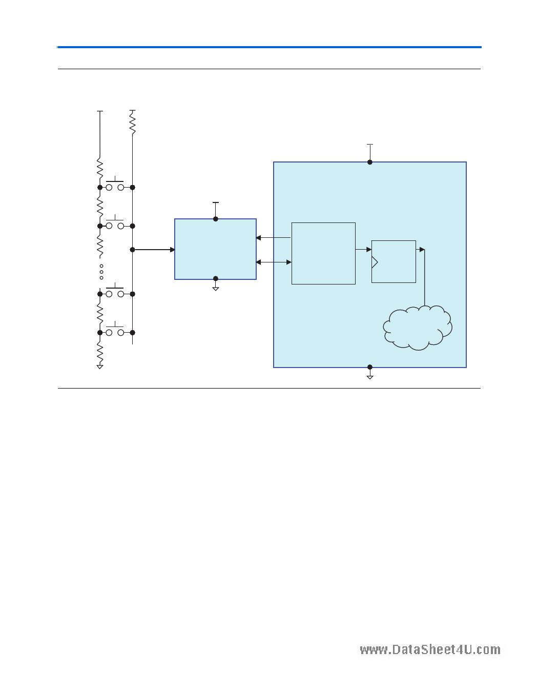
In Figure 3, a resistor stack goes between VCC and GND. When a switch is
closed, it connects the respective resistor tap to the serial analog-to-digital
converter. You can program a CPLD to read the voltage sensed from the
switch array. The CPLD drives the analog-to-digital converter with the
right commands and protocol to capture the data and place it in a parallel
register. This approach makes for a very simple switch array that only
requires three wires: VCC, GND, and Sense.
As shown in Figure 4, it is very easy to integrate the series resistor into a
single-layer membrane switch. You can make the traces in the membrane
switch PCB resistive in many ways. The trace width can be made very
narrow, a more resistive conductor can be used in resistor segments, and
the trace can be etched thinner to increase resistance.
Altera Corporation
5
Preliminary
5 Page 
www.datasheet4u.com
New Two-Wire Keypad Decider
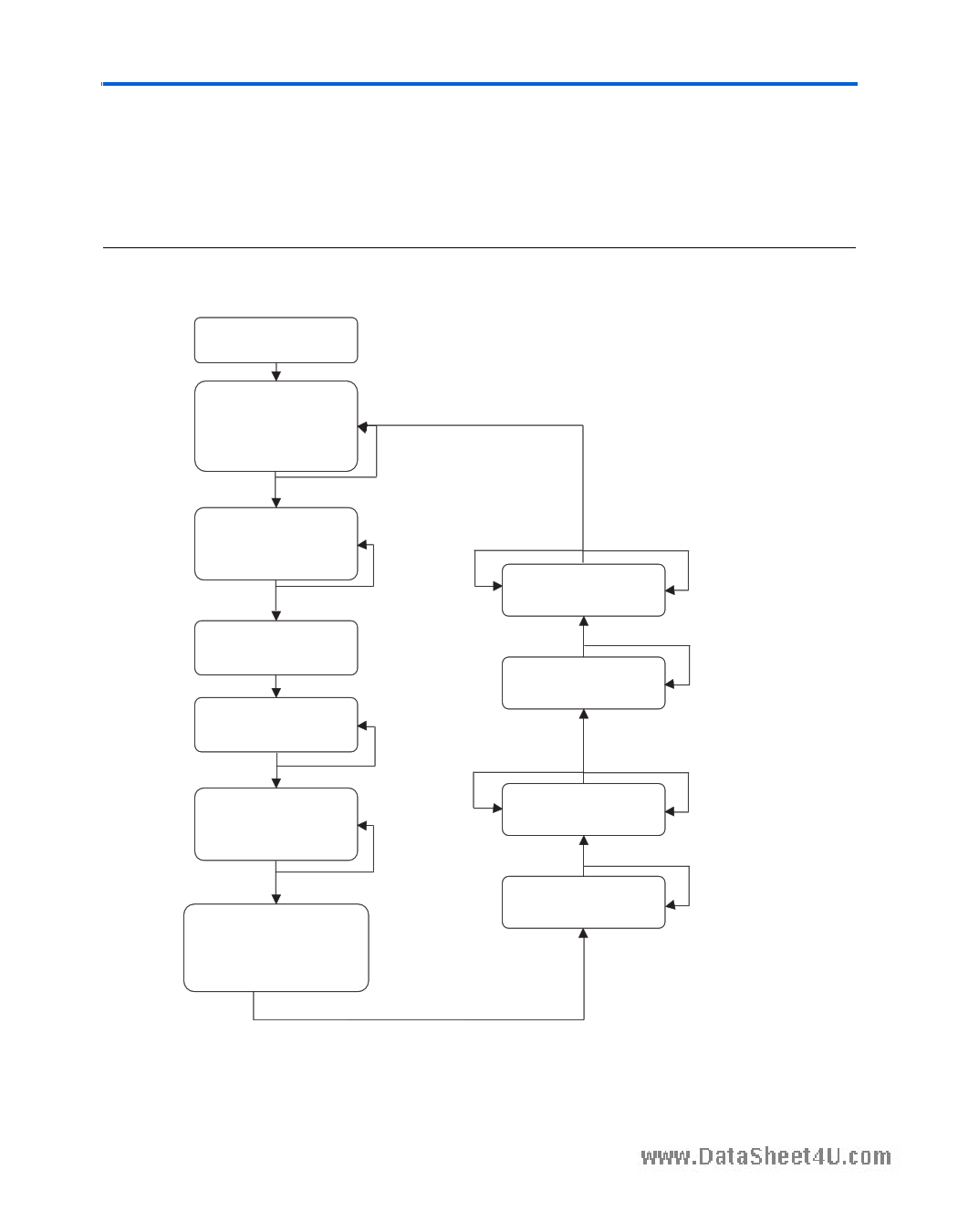
The flow chart in Figure 7 describes the operation of the control block
from Figure 5 in detail. The control block controls the timing of the
sample measurement, the reference measurement, and the debounce of
the switches. This diagram only specifies active signal outputs. All
signals not specified are in a low or inactive state.
Figure 7. Control Block State Machine for a Two-Pin Keypad Decode(1)
POR Reset
Sense = Z
PreCharge = 1
RefReset = 1
SampleReset = 1
100 μS
Sense = Z
PreCharge = Z
RefEnable = 1
PreCharge = 0
Sense = Z
PreCharge = Z
Sense = Z
PreCharge = 1
100 μS
Sense = 0
PreCharge = Z
SampleEnable = 1
PreCharge = 0
Sense = Z
PreCharge = Z
SwitchLoad = 1
Switch = Sample*N/Ref
< 100 μS
Sense = 0* > 100μS
Sense = 1* > 100μS
PreCharge = 1
Sense = Z
PreCharge = Z
< 100 μS
Sense = 0
Sense = Z
PreCharge = Z
Sense = 1
< 10 μS
Sense = 1* > 100 μS
Sense = 0* > 100 μS
PreCharge = 1
Sense = Z
PreCharge = Z
Sense = 1
Sense = Z
PreCharge = Z
< 100 μS
Sense = 0
Note to Figure 7:
(1) Outputs: PreCharge, Sense, RefReset, RefEnable, SampleReset, SampleEnable, SwitchLoad, TimerReset, Inputs,
PreCharge, Sense, 100 μS.
Altera Corporation
11
Preliminary
11 Page | ||
| Páginas | Total 15 Páginas | |
| PDF Descargar | [ Datasheet AN-426.PDF ] | |
Hoja de datos destacado
| Número de pieza | Descripción | Fabricantes |
| AN-426 | Analog Keyboard Encoder | Altera |
| Número de pieza | Descripción | Fabricantes |
| SLA6805M | High Voltage 3 phase Motor Driver IC. |
Sanken |
| SDC1742 | 12- and 14-Bit Hybrid Synchro / Resolver-to-Digital Converters. |
Analog Devices |
|
DataSheet.es es una pagina web que funciona como un repositorio de manuales o hoja de datos de muchos de los productos más populares, |
| DataSheet.es | 2020 | Privacy Policy | Contacto | Buscar |
