|
|
PDF LT8410 Data sheet ( Hoja de datos )
| Número de pieza | LT8410 | |
| Descripción | Ultralow Power Boost Converter | |
| Fabricantes | Linear Technology Corporation | |
| Logotipo |  |
|
Hay una vista previa y un enlace de descarga de LT8410 (archivo pdf) en la parte inferior de esta página. Total 16 Páginas | ||
|
No Preview Available !
FEATURES
n Ultralow Quiescent Current
8.5μA in Active Mode
0μA in Shutdown Mode
n Comparator Built into SHDN pin
www.DataShneetL4Uo.wcoNmoise Control Scheme
n Adjustable FB reference voltage
n Wide Input Range: 2.5V to 16V
n Wide Output Range : Up to 40V
n Integrated Power NPN Switch
25mA Current Limit (LT8410)
8mA Current Limit (LT8410-1)
n Integrated Schottky Diode
n Integrated Output Disconnect
n High Value (12.4M/0.4M) Feedback Resistors
Integrated
n Built in Soft-Start (Optional Capacitor from VREF to
GND)
n Overvoltage Protection for CAP and VOUT pins
n Tiny 8-Pin 2mm × 2mm DFN package
APPLICATIONS
n Sensor Power
n RF Mems Relay Power
n General Purpose Bias
LT8410/LT8410-1
Ultralow Power Boost
Converter with Output
Disconnect
DESCRIPTION
The LT®8410/LT8410-1 are ultralow power boost converters
with integrated power switch, Schottky diode and output
disconnect circuitry. The parts control power delivery by
varying both the peak inductor current and switch off-
time. This control scheme results in low output voltage
ripple as well as high efficiency over a wide load range.
The quiescent current is a low 8.5μA, which is further
reduced to 0μA in shutdown. The internal disconnect
circuitry allows the output voltage to be blocked from
the input during shutdown. High value (12.4M/0.4M)
resistors are integrated on chip for output voltage detection,
significantly reducing input referred quiescent current.
The LT8410/-1 also features a comparator built into the
SHDN pin, over voltage protection for the CAP and VOUT
pins, built in soft-start and comes in a tiny 8-pin 2mm ×
2mm DFN package.
L, LT, LTC and LTM are registered trademarks of Linear Technology Corporation. Hot Swap
is a trademark of Linear Technology Corporation. All other trademarks are the property of their
respective owners. Protected by U.S. Patents including 5481178, 6580258, 6304066, 6127815,
6498466, 6611131.
TYPICAL APPLICATION
General Purpose Bias with Wide Input Voltage
VIN
2.5V to 16V
100μH
2.2μF
CHIP
ENABLE
SW CAP
VCC VOUT
LT8410
SHDN VREF
GND FBP
*HIGHER VALUE CAPACITOR IS REQUIRED
WHEN THE VIN IS HIGHER THAN 5V
0.1μF
VOUT = 16V
0.1μF*
604K
412K
0.1μF
8410-1 TA01a
Output Voltage Ripple
vs Load Current
10
VIN = 3.6V
8
6
4
2
0
0.01
0.1 1
LOAD CURRENT (mA)
10
8410-1 TA02
Efficiency vs Load Current
100
VIN = 12V
90
80 VIN = 5V
VIN = 3.6V
70
60
50
40
0.01
0.1 1
10
LOAD CURRENT (mA)
100
8410-1 TA03
84101f
1
1 page 
TYPICAL PERFORMANCE CHARACTERISTICS
LT8410/LT8410-1
LT8410 Switching Waveform
at No Load
VOUT VOLTAGE
2mV/DIV
AC COUPLED
SW VOLTAGE
10V/DIV
www.DataSheet4U.com INDUCTOR
CURRENT
10mA/DIV
VCC = 3.6V
VOUT = 16V
50μs/DIV
8410-1 G13
LT8410 Switching Waveform
at 0.5mA Load
VOUT VOLTAGE
10mV/DIV
AC COUPLED
SW VOLTAGE
10V/DIV
INDUCTOR
CURRENT
20mA/DIV
VCC = 3.6V
VOUT = 16V
2μs/DIV
8410-1 G14
LT8410 Switching Waveform
at 3mA Load
VOUT VOLTAGE
10mV/DIV
AC COUPLED
SW VOLTAGE
10V/DIV
INDUCTOR
CURRENT
20mA/DIV
VCC = 3.6V
VOUT = 16V
500ns/DIV
8410-1 G15
Line Regulation
0.3
VOUT = 16V
0.25
0.2
0.15
0.1
0.05
0
0 4 8 12 16
VCC VOLTAGE (V)
8410-1 G17
UVLO vs Temperature
2.6
2.4
VCC RISING
2.2
VCC FALLING
2
1.8
1.6
1.4
– 40
0 40 80
TEMPERATURE (°C)
120
8410-1 G16
SHDN Minimum Input Voltage
High vs Temperature
1.5
1.4
SHDN RISING
1.3
SHDN FALLING
1.2
1.1
1
– 40
0 40 80
TEMPERATURE (°C)
120
8410-1 G18
84101f
5
5 Page 
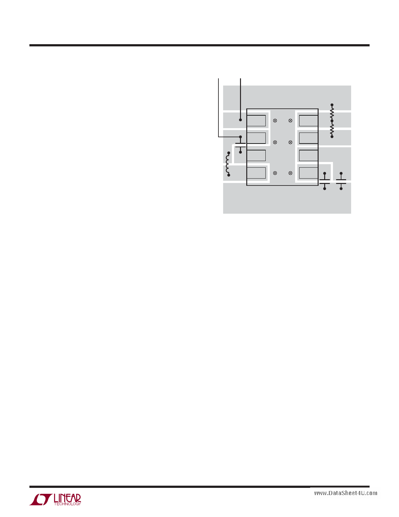
APPLICATIONS INFORMATION
Board Layout Considerations
As with all switching regulators, careful attention must
be paid to the PCB layout and component placement. To
maximize efficiency, switch rise and fall times are made as
short as possible. To prevent electromagnetic interference
(EMI) problems, proper layout of the high frequency
switching path is essential. The voltage signal of the SW pin
has sharp rising and falling edges. Minimize the length and
www.DataShaereet4aUo.cfoamll traces connected to the SW pin and always use
a ground plane under the switching regulator to minimize
interplane coupling. In addition, the FBP pin and VREF pin
are sensitive to noise. Minimize the length and area of all
traces to these two pins is recommended. Recommended
component placement is shown in Figure 3.
LT8410/LT8410-1
VIN SHDN
SHDN
VCC
GND
SW
FBP
VREF
CAP
GND
VOUT
CAPACITOR GROUNDS MUST BE
RETURNED DIRECTLY TO IC GROUND
8410-1 F03
Figure 3. Recommended Board Layout
84101f
11
11 Page | ||
| Páginas | Total 16 Páginas | |
| PDF Descargar | [ Datasheet LT8410.PDF ] | |
Hoja de datos destacado
| Número de pieza | Descripción | Fabricantes |
| LT8410 | Ultralow Power Boost Converter | Linear Technology Corporation |
| LT8410-1 | Ultralow Power Boost Converter | Linear Technology Corporation |
| LT8415 | Ultralow Power Boost Converter | Linear Technology |
| Número de pieza | Descripción | Fabricantes |
| SLA6805M | High Voltage 3 phase Motor Driver IC. |
Sanken |
| SDC1742 | 12- and 14-Bit Hybrid Synchro / Resolver-to-Digital Converters. |
Analog Devices |
|
DataSheet.es es una pagina web que funciona como un repositorio de manuales o hoja de datos de muchos de los productos más populares, |
| DataSheet.es | 2020 | Privacy Policy | Contacto | Buscar |
