|
|
|
PDF CS5504 Data sheet ( Hoja de datos )
| Número de pieza | CS5504 | |
| Descripción | 20-Bit A/D Converter | |
| Fabricantes | Cirrus Logic | |
| Logotipo | ||
Hay una vista previa y un enlace de descarga de CS5504 (archivo pdf) en la parte inferior de esta página. Total 24 Páginas | ||
|
No Preview Available !
CCDCSB5S55550504044
EvaluLLaotoiwown-PpBoowowaeerrd,,22f0o0-r-BbCiittSAA5/5/DD04CCAoon/nDveCrotenrverter
Features
l Delta-sigma A/D Converter
- 20-bit, No Missing Codes
- Linearity Error: ±0.0007%FS
l 2 Differential Inputs
- Pin-selectable Unipolar/Bipolar Ranges
www.DataSheet4U- .cComommon Mode Rejection
105 dB @ dc
120 dB @ 50, 60 Hz
l Either 5V or 3.3V Digital Interface
l On-chip Self-calibration Circuitry
l Output Update Rates up to 200/Sps
l Low Power Consumption: 4.4 mW
Description
The CS5504 is a 2-channel, fully differential 20-bit, seri-
al-output CMOS A/D converter. The CS5504 uses
charge-balanced (delta-sigma) techniques to provide a
low cost, high-resolution measurement at output word
rates up to 200 samples per second.
The on-chip digital filter offers superior line rejection at
50 Hz and 60 Hz when the device is operated from a
32.768 kHz clock (output word rate = 20 Sps).
The CS5504 has on-chip self-calibration circuitry which
can be initiated at any time or temperature to ensure
minimum offset and full-scale errors.
Low power, high-resolution and small package size
make the CS5504 an ideal solution for loop-powered
transmitters, panel meters, weigh scales and battery-
powered instruments.
ORDERING INFORMATION
See page 23.
CS5504-BS -40° to +85° C 20-pin SOIC
I
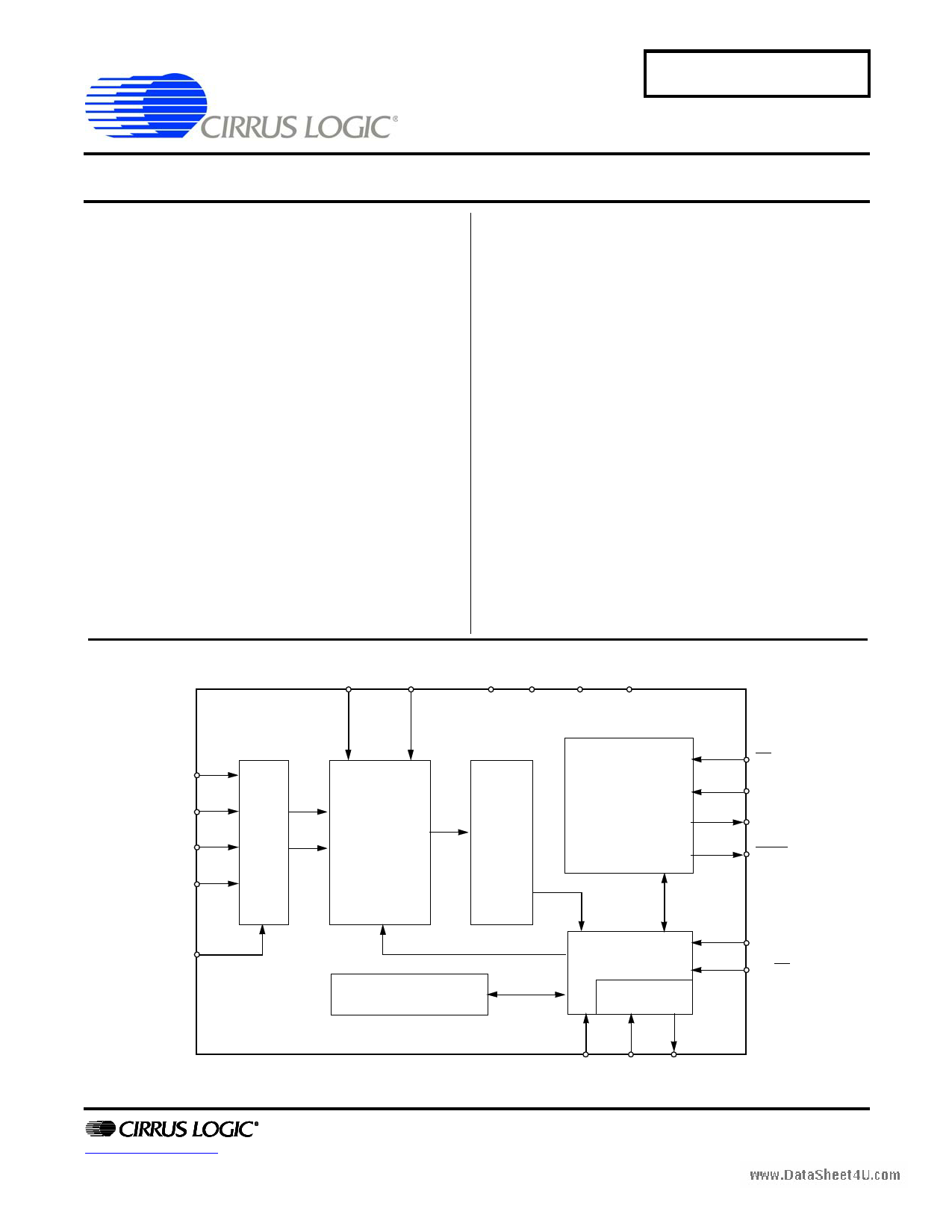
VREF+
12
VREF-
13
VA+ VA- DGND VD+
14 15
16 17
AIN1+
AIN1-
8
10
AIN2+
AIN2-
9
11
MUX
4th-Order
Delta-Sigma
Modulator
Digital
Filter
Serial
Interface
Logic
2
CS
18 SCLK
19
SDATA
20
DRDY
A0 1
Calibration SRAM
Calibration µC
OSC
3 56
CONV XIN XOUT
4 CAL
7 BP/UP
Cirrus Logic, Inc.
PCh.rtOtyps.:/tB/awol wxSw1e7m.c8iir4cr7uo,snA.dcuousmctitno,rTPerxoadsu7c8ts76D0ivision
(512) 445 7222 FAX: (512) 445 7581
http://www.crystal.com
Copyright © CirrCuospLyoriggich,t I©ncC. i2rr0u0s5Logic, Inc. 1997
(All Rights Rese(rAvell dR)ights Reserved)
MAUARG ‘905
DSA1U2G6F‘1025
DS126DB12
1 page 
CS5504
CS5504
3.3V SWITCHING CHARACTERISTICS (TA = TMIN to TMAX; VA+ = 5V ± 10%; VD+ = 3.3V ±
5%; VA- = -5V ± 10%; Input Levels: Logic 0 = 0V, Logic 1 = VD+; CL = 50 pF.) (Note 2)
Parameter
Symbol Min Typ Max Units
Master Clock Frequency
Internal Oscillator
External Clock
Master Clock Duty Cycle
Rise Times:
Any Digital Input (Note 9)
Any Digital Output
Fall Times:
www.DataSheet4U.com
Any Digital Input (Note 9)
Any Digital Output
Start-Up
Power-On Reset Period
(Note 10)
Oscillator Start-up Time
XTAL = 32.768 kHz (Note 11)
Wake-up Period
(Note 12)
Calibration
CONV Pulse Width (CAL=1)
(Note 13)
CONV and CAL High to Start of Calibration
Start of Calibration to End of Calibration
Conversion
Set Up Time
A0 to CONV High
Hold Time
A0 after CONV High
CONV Pulse Widh
CONV High to Start of Conversion
Set Up Time
BP/UP stable prior to DRDY falling
Hold Time
BP/UP stable after DRDY falls
Start of Conversion to End of Conversion
(Note 14)
XIN
fclk
trise
tfall
tres
tosu
twup
tccw
tscl
tcal
tsac
thca
tcpw
tscn
tbus
tbuh
tcon
30.0 32.768 53.0 kHz
30 - 330 kHz
40 - 60 %
- - 1.0 µs
- 50 - ns
- - 1.0 µs
- 20 - ns
- 10 -
- 500 -
- 1800/fclk -
ms
ms
s
100 -
- ns
- - 2/fclk+200 ns
- 3246/fclk -
s
50
100
100
-
82/fclk
0
-
--
--
--
- 2/fclk+200
--
--
1624/fclk
-
ns
ns
ns
ns
s
ns
s
DS126F12
5
5 Page 
CS5504
CS5504
output code. The only difference is that in bipo-
lar mode the on-chip microcontroller offsets the
computed output word by a code value of
8000H. This means that the bipolar measure-
ment range is not calibrated from full scale
positive to full scale negative. Instead it is cali-
brated from the bipolar zero scale point to full
scale positive. The slope factor is then extended
below bipolar zero to accommodate the negative
input signals. The converter can be used to con-
www.DataSheevt4eUr.ctomboth unipolar and bipolar signals by
changing the BP/UP pin. Recalibration is not re-
quired when switching between unipolar and
bipolar modes.
At the end of the calibration cycle, the on-chip
micro controller checks the logic state of the
CONV signal. If the CONV input is low the de-
vice will enter the standby mode where it waits
for further instruction. If the CONV signal is
high at the end of the calibration cycle, the con-
verter will enter the conversion state and
perform a conversion on the input channel. The
CAL signal can be returned low any time after
calibration is initiated. CONV can also be re-
turned low, but it should never be taken low and
then taken back high until the calibration period
has ended and the converter is in the standby
state. If CONV is taken low and then high
again with CAL high while the converter is cali-
brating, the device will interrupt the current
calibration cycle and start a new one. If CAL is
taken low and CONV is taken low and then high
during calibration, the calibration cycle will
continue as the conversion command is disre-
garded. The state of BP/UP is not important
during calibrations.
If an "end of calibration" signal is desired, pulse
the CAL signal high while leaving the CONV
signal high continuously. Once the calibration is
completed, a conversion will be performed. At
the end of the conversion, DRDY will fall to in-
dicate the first valid conversion after the
calibration has been completed.
DS126F12
Conversion
The conversion state can be entered at the end of
the calibration cycle, or whenever the converter
is idle in the standby mode. If CONV is taken
high to initiate a calibration cycle ( CAL also
high), and remains high until the calibration cy-
cle is completed (CAL is taken low after CONV
transitions high), the converter will begin a con-
version upon completion of the calibration
period. The device will perform a conversion on
the input channel selected by A0 when CONV
transitions high. Table 1 indicates the multi-
plexer channel selection truth table.
A0 Channel Addressed
0 AIN1
1 AIN2
Table 1. Multiplexer Truth Table
The A0 input is latched internal to the CS5504
when CONV rises. A0 has internal pull-down
circuits which default the multiplexer to channel
AIN1.
The BP/UP pin is not a latched input. The
BP/UP pin controls how the output word from
the digital filter is processed. In bipolar mode
the output word computed by the digital filter is
offset by 80000H (see Understanding Converter
Calibration). BP/UP can be changed after a con-
version is started as long as it is stable for 82
clock cycles of the conversion period prior to
DRDY falling. If one wishes to intermix meas-
urement of bipolar and unipolar signals on
various input channels, it is best to switch the
BP/UP pin immediately after DRDY falls and
leave BP/UP stable until DRDY falls again.
The digital filter in the CS5504 has a Finite Im-
pulse Response and is designed to settle to full
accuracy in one conversion time.
If CONV is left high, the CS5504 will perform
continuous conversions. The conversion time
will be 1622 clock cycles. If conversion is initi-
11
11 Page | ||
| Páginas | Total 24 Páginas | |
| PDF Descargar | [ Datasheet CS5504.PDF ] | |
Hoja de datos destacado
| Número de pieza | Descripción | Fabricantes |
| CS5501 | (CS5501 / CS5503) Measurement A/D Converter | Crystal |
| CS5503 | (CS5501 / CS5503) Measurement A/D Converter | Crystal |
| CS5504 | 20-Bit A/D Converter | Cirrus Logic |
| CS5505 | 16-Bit and 20-Bit A/D Converters | Crystal |
| Número de pieza | Descripción | Fabricantes |
| SLA6805M | High Voltage 3 phase Motor Driver IC. |
Sanken |
| SDC1742 | 12- and 14-Bit Hybrid Synchro / Resolver-to-Digital Converters. |
Analog Devices |
|
DataSheet.es es una pagina web que funciona como un repositorio de manuales o hoja de datos de muchos de los productos más populares, |
| DataSheet.es | 2020 | Privacy Policy | Contacto | Buscar |