|
|
|
PDF LM2931 Data sheet ( Hoja de datos )
| Número de pieza | LM2931 | |
| Descripción | Low Dropout Regulators | |
| Fabricantes | National Semiconductor | |
| Logotipo | ||
1. LM2931 Hay una vista previa y un enlace de descarga de LM2931 (archivo pdf) en la parte inferior de esta página. Total 18 Páginas | ||
|
No Preview Available !
June 2005
LM2931
Series Low Dropout Regulators
General Description
The LM2931 positive voltage regulator features a very low
quiescent current of 1mA or less when supplying 10mA loads.
This unique characteristic and the extremely low input-output
differential required for proper regulation (0.2V for output cur-
rents of 10mA) make the LM2931 the ideal regulator for
standby power systems. Applications include memory stand-
by circuits, CMOS and other low power processor power
supplies as well as systems demanding as much as 100mA
of output current.
Designed originally for automotive applications, the LM2931
and all regulated circuitry are protected from reverse battery
installations or 2 battery jumps. During line transients, such
as a load dump (60V) when the input voltage to the regulator
can momentarily exceed the specified maximum operating
voltage, the regulator will automatically shut down to protect
both internal circuits and the load. The LM2931 cannot be
harmed by temporary mirror-image insertion. Familiar regu-
lator features such as short circuit and thermal overload pro-
tection are also provided.
The LM2931 family includes a fixed 5V output (±3.8% toler-
ance for A grade) or an adjustable output with ON/OFF pin.
Both versions are available in a TO-220 power package,
TO-263 surface mount package, and an 8-lead surface mount
package. The fixed output version is also available in the
TO-92 plastic and 6-Bump micro SMD packages.
Features
■ Very low quiescent current
■ Output current in excess of 100 mA
■ Input-output differential less than 0.6V
■ Reverse battery protection
■ 60V load dump protection
■ −50V reverse transient protection
■ Short circuit protection
■ Internal thermal overload protection
■ Mirror-image insertion protection
■ Available in TO-220, TO-92, TO-263, SO-8 or 6-Bump mi-
cro SMD packages
■ Available as adjustable with TTL compatible switch
■ See AN-1112 for micro SMD considerations
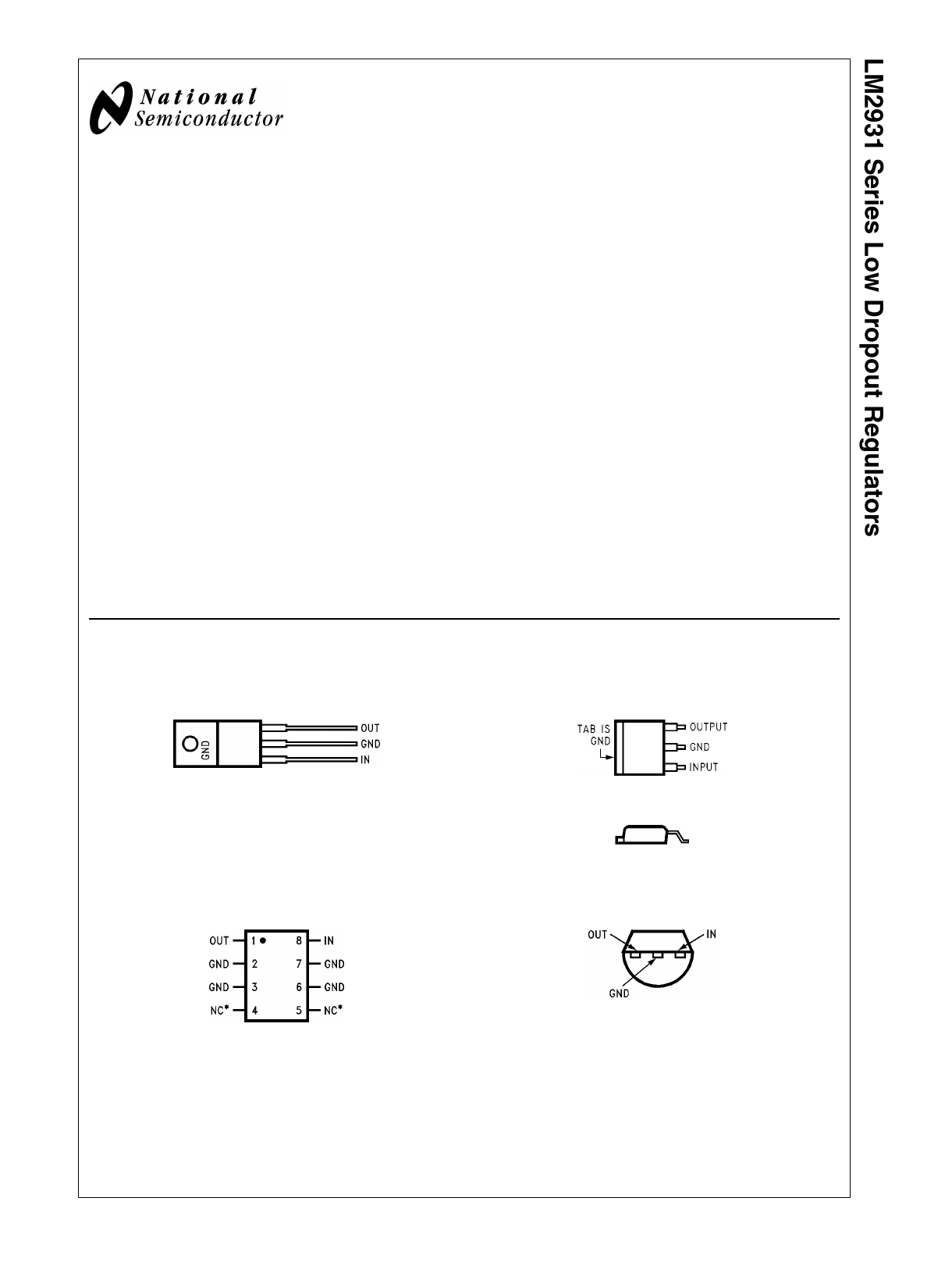
Connection Diagrams
FIXED VOLTAGE OUTPUT
TO-220 3-Lead Power Package
TO-263 Surface-Mount Package
Front View
525406
8-Pin Surface Mount
525411
Top View
525412
Side View
TO-92 Plastic Package
525407
*NC = Not internally connected. Must be electrically isolated from the rest of
the circuit for the micro SMD package.
Top View
525408
Bottom View
© 2006 National Semiconductor Corporation 5254
www.national.com
1 page 
Absolute Maximum Ratings (Note 1)
If Military/Aerospace specified devices are required,
please contact the National Semiconductor Sales Office/
Distributors for availability and specifications.
Input Voltage
Operating Range
Overvoltage Protection
LM2931A, LM2931C (Adjustable)
26V
60V
LM2931
Internal Power Dissipation
(Notes 2, 4)
Operating Ambient Temperature
Range
Maximum Junction Temperature
Storage Temperature Range
Lead Temp. (Soldering, 10 seconds)
ESD Tolerance (Note 5)
50V
Internally Limited
−40°C to +85°C
125°C
−65°C to +150°C
230°C
2000V
Electrical Characteristics for Fixed 3.3V Version
VIN = 14V, IO = 10mA, TJ = 25°C, C2 = 100μF (unless otherwise specified) (Note 2)
Parameter
Conditions
Output Voltage
4V ≤ VIN ≤ 26V, IO = 100 mA
−40°C ≤ TJ ≤ 125°C
Line Regulation
4V ≤ VIN ≤ 26V
Load Regulation
5mA ≤ IO ≤ 100mA
Output Impedance
100mADC and 10mArms,
100Hz - 10kHz
Quiescent Current
IO ≤ 10mA, 4V ≤ VIN ≤ 26V
−40°C ≤ TJ ≤ 125°C
IO = 100mA, VIN = 14V, TJ = 25°C
Output Noise Voltage
10Hz -100kHz, COUT = 100μF
Long Term Stability
Ripple Rejection
fO = 120Hz
Dropout Voltage
IO = 10mA
IO = 100mA
Maximum Operational Input
Voltage
Maximum Line Transient
RL = 500Ω, VO ≤ 5.5V,
T = 1ms, τ ≤ 100ms
Reverse Polarity Input Voltage, DC VO ≥ −0.3V, RL = 500Ω
Reverse Polarity Input Voltage,
Transient
T = 1ms, τ ≤ 100ms, RL = 500Ω
LM2931-3.3
Typ Limit
(Note 3)
3.3 3.465
3.135
3.630
2.970
4 33
10 50
200
0.4 1.0
15
330
13
80
0.05
0.30
33
70
−30
−80
0.2
0.6
26
50
−15
−50
Units
VMAX
VMIN
VMAX
VMIN
mVMAX
mVMAX
mΩ
mAMAX
mA
μVrms
mV/1000 hr
dB
VMAX
VMIN
VMIN
VMIN
VMIN
5 www.national.com
5 Page 
Maximum Power Dissipation
(TO-263) (Note 4)
On/Off Threshold
525434
Output Capacitor ESR
525435
525436
11 www.national.com
11 Page | ||
| Páginas | Total 18 Páginas | |
| PDF Descargar | [ Datasheet LM2931.PDF ] | |
Hoja de datos destacado
| Número de pieza | Descripción | Fabricantes |
| LM293 | Low power dual voltage comparator | NXP Semiconductors |
| LM293 | LOWPOWER DUAL VOLTAGE COMPARATORS | STMicroelectronics |
| LM293 | Low Power Low Offset Voltage Dual Comparators | National Semiconductor |
| LM293 | LMx93 LM2903 Dual Differential Comparators (Rev. Y) | Texas Instruments |
| Número de pieza | Descripción | Fabricantes |
| SLA6805M | High Voltage 3 phase Motor Driver IC. |
Sanken |
| SDC1742 | 12- and 14-Bit Hybrid Synchro / Resolver-to-Digital Converters. |
Analog Devices |
|
DataSheet.es es una pagina web que funciona como un repositorio de manuales o hoja de datos de muchos de los productos más populares, |
| DataSheet.es | 2020 | Privacy Policy | Contacto | Buscar |