|
|
|
PDF 7650SCB Data sheet ( Hoja de datos )
| Número de pieza | 7650SCB | |
| Descripción | ICL7650SCB | |
| Fabricantes | Intersil Corporation | |
| Logotipo | ||
Hay una vista previa y un enlace de descarga de 7650SCB (archivo pdf) en la parte inferior de esta página. Total 14 Páginas | ||
|
No Preview Available !
TM
Data Sheet
ICL7650S
April 2000
File Number 2920.5
2MHz, Super Chopper-Stabilized
Operational Amplifier
The ICL7650S Super Chopper-Stabilized Amplifier offers
exceptionally low input offset voltage and is extremely stable
with respect to time and temperature. It is a direct
replacement for the industry-standard ICL7650 offering
improved input offset voltage, lower input offset voltage
temperature coefficient, reduced input bias current, and
wider common mode voltage range. All improvements are
www.DataSheheigt4hUli.gchotmed in bold italics in the Electrical Characteristics
section. Critical parameters are guaranteed over the
entire commercial temperature range.
Intersil’s unique CMOS chopper-stabilized amplifier circuitry
is user-transparent, virtually eliminating the traditional
chopper amplifier problems of intermodulation effects,
chopping spikes, and overrange lockup.
The chopper amplifier achieves its low offset by comparing
the inverting and non-inverting input voltages in a nulling
amplifier, nulled by alternate clock phases. Two external
capacitors are required to store the correcting potentials on
the two amplifier nulling inputs; these are the only external
components necessary.
The clock oscillator and all the other control circuitry is
entirely self-contained. However the 14 lead version includes
a provision for the use of an external clock, if required for a
particular application. In addition, the ICL7650S is internally
compensated for unity-gain operation.
Features
• Guaranteed Max Input Offset Voltage for All Temperature
Ranges
• Low Long-Term and Temperature Drifts of Input Offset
Voltage
• Guaranteed Max Input Bias Current. . . . . . . . . . . . . .10pA
• Extremely Wide Common Mode
Voltage Range . . . . . . . . . . . . . . . . . . . . . . . +3.5V to -5V
• Reduced Supply Current . . . . . . . . . . . . . . . . . . . . . . 2mA
• Guaranteed Minimum Output Source/Sink Current
• Extremely High Gain . . . . . . . . . . . . . . . . . . . . . . . .150dB
• Extremely High CMRR and PSRR . . . . . . . . . . . . . .140dB
• High Slew Rate. . . . . . . . . . . . . . . . . . . . . . . . . . . .2.5V/µs
• Wide Bandwidth . . . . . . . . . . . . . . . . . . . . . . . . . . . . 2MHz
• Unity-Gain Compensated
• Clamp Circuit to Avoid Overload Recovery Problems and
Allow Comparator Use
• Extremely Low Chopping Spikes at Input and Output
• Improved, Direct Replacement for Industry-Standard
ICL7650 and other Second-Source Parts
Ordering Information
PART NUMBER
ICL7650SCPA-1
TEMP.
RANGE
(oC)
PACKAGE
0 to 70 8 Ld PDIP
ICL7650SCPD
ICL7650SCBA-1
ICL7650SCTV-1
0 to 70
0 to 70
0 to 70
14 Ld PDIP
8 Ld SOIC
8 Pin Metal Can
PKG.
NO.
E8.3
E14.3
M8.15
T8.C
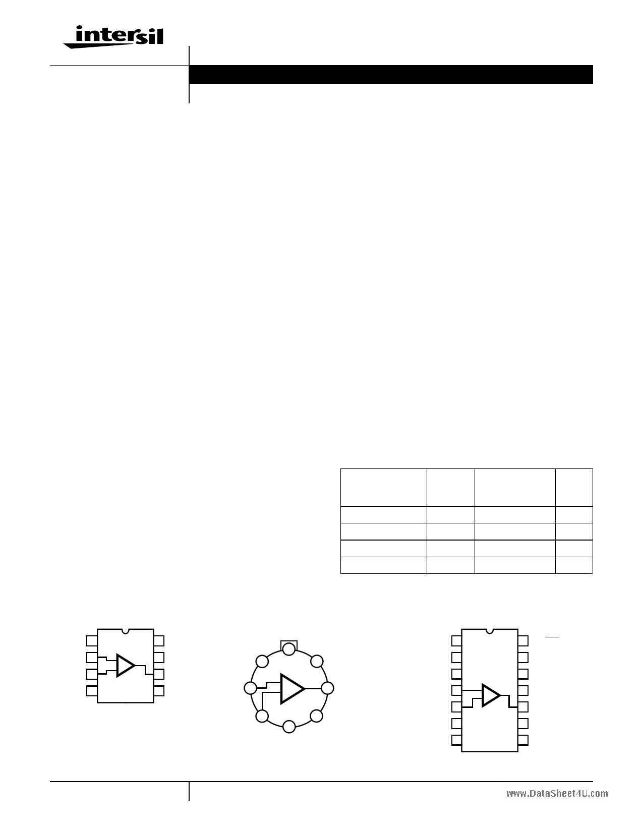
Pinouts
ICL7650S (PDIP, SOIC)
TOP VIEW
CEXTA 1
-IN 2
+IN 3
V- 4
-
+
8 CEXTB
7 V+
6 OUTPUT
5 CRETN
ICL7650S (METAL CAN)
TOP VIEW
CEXTB
CEXTA 1
8
7 V+/CASE
-IN 2
-
+
6 OUTPUT
+IN 3
5 CRETN
4
V-
ICL7650S (PDIP)
TOP VIEW
CEXTB 1
CEXTA 2
NC (GUARD) 3
-IN 4
+IN 5
NC (GUARD) 6
V- 7
-
+
14 INT/EXT
13 EXT CLK IN
12 INT CLK OUT
11 V+
10 OUTPUT
9 OUT CLAMP
8 CRETN
1 CAUTION: These devices are sensitive to electrostatic discharge; follow proper IC Handling Procedures.
1-888-INTERSIL or 321-724-7143 | Intersil and Design is a trademark of Intersil Corporation. | Copyright © Intersil Corporation 2000
1 page 
ICL7650S
desired 50% input switching duty cycle. Since the capacitors
are charged only when EXT CLOCK IN is high, a 50% - 80%
positive duty cycle is recommended, especially for higher
frequencies. The external clock can swing between V+ and V-.
The logic threshold will be at about 2.5V below V+. Note also
that a signal of about 400 Hz, with a 70% duty cycle, will be
present at the EXT CLOCK IN pin with INT/EXT high or open.
This is the internal clock signal before being fed to the divider.
In those applications where a strobe signal is available, an
alternate approach to avoid capacitor misbalancing during
overload can be used. If a strobe signal is connected to EXT
CLK IN so that it is low during the time that the overload
signal is applied to the amplifier, neither capacitor will be
www.DataShecehta4Urg.ecodm. Since the leakage at the capacitor pins is quite low
at room temperature, the typical amplifier will drift less than
10µV/s, and relatively long measurements can be made with
little change in offset.
COMPONENT SELECTION
The two required capacitors, CEXTA and CEXTB, have
optimum values depending on the clock or chopping
frequency. For the preset internal clock, the correct value is
0.1µF, and to maintain the same relationship between the
chopping frequency and the nulling time constant this value
should be scaled approximately in proportion if an external
clock is used. A high quality film type capacitor such as
mylar is preferred, although a ceramic or other lower-grade
capacitor may prove suitable in many applications. For
quickest settling on initial turn-on, low dielectric absorption
capacitors (such as polypropylene) should be used. With
ceramic capacitors, several seconds may be required to
settle to 1µV.
STATIC PROTECTION
All device pins are static-protected by the use of input diodes.
However, strong static fields and discharges should be avoided,
as they can cause degraded diode junction characteristics,
which may result in increased input-leakage currents.
LATCHUP AVOIDANCE
Junction-isolated CMOS circuits inherently include a parasitic
4-layer (PNPN) structure which has characteristics similar to
an SCR. Under certain circumstances this junction may be
triggered into a low-impedance state, resulting in excessive
supply current. To avoid this condition, no voltage greater than
0.3V beyond the supply rails should be applied to any pin. In
general, the amplifier supplies must be established either at
the same time or before any input signals are applied. If this is
not possible, the drive circuits must limit input current flow to
under 1mA to avoid latchup, even under fault conditions.
OUTPUT STAGE/LOAD DRIVING
The output circuit is a high-impedance type (approximately
18kΩ), and therefore with loads less than this value, the
chopper amplifier behaves in some ways like a
transconductance amplifier whose open-loop gain is
proportional to load resistance. For example, the open-loop
gain will be 17dB lower with a 1kΩ load than with a 10kΩ
load. If the amplifier is used strictly for DC, this lower gain is
of little consequence, since the DC gain is typically greater
than 120dB even with a 1kΩ load. However, for wideband
applications, the best frequency response will be achieved
with a load resistor of 10kΩ or higher. This will result in a
smooth 6dB/octave response from 0.1Hz to 2MHz, with
phase shifts of less than 10 degrees in the transition region
where the main amplifier takes over from the null amplifier.
THERMO-ELECTRIC EFFECTS
The ultimate limitations to ultra-high precision DC amplifiers are
the thermo-electric or Peltier effects arising in thermocouple
junctions of dissimilar metals, alloys, silicon, etc. Unless all
junctions are at the same temperature, thermoelectric voltages
typically around 0.1µV/oC, but up to tens of mV/oC for some
materials, will be generated. In order to realize the extremely
low offset voltages that the chopper amplifier can provide, it is
essential to take special precautions to avoid temperature
gradients. All components should be enclosed to eliminate air
movement, especially that caused by power-dissipating
elements in the system. Low thermoelectric-efficient
connections should be used where possible and power supply
voltages and power dissipation should be kept to a minimum.
High-impedance loads are preferable, and good separation
from surrounding heat-dissipating elements is advisable.
GUARDING
Extra care must be taken in the assembly of printed circuit
boards to take full advantage of the low input currents of the
ICL7650S. Boards must be thoroughly cleaned with TCE or
alcohol and blown dry with compressed air. After cleaning,
the boards should be coated with epoxy or silicone rubber to
prevent contamination.
Even with properly cleaned and coated boards, leakage
currents may cause trouble, particularly since the input pins
are adjacent to pins that are at supply potentials. This
leakage can be significantly reduced by using guarding to
lower the voltage difference between the inputs and adjacent
metal runs. Input guarding of the 8-pin TO-99 package is
accomplished by using a 10-lead pin circle, with the leads of
the device formed so that the holes adjacent to the inputs
are empty when it is inserted in the board. The guard, which
is a conductive ring surrounding the inputs, is connected to a
low impedance point that is at approximately the same
voltage as the inputs. Leakage currents from high-voltage
pins are then absorbed by the guard.
5
5 Page 
ICL7650S
Dual-In-Line Plastic Packages (PDIP)
INDEX
AREA
N
12 3
-A-
BASE
PLANE
SEATING
PLANE
D1
B1
www.DataSheet4U.com
B
E1
N/2
-B-
D
-C- A2 A
L
D1
e
A1
eC
0.010 (0.25) M C A B S
E
CL
eA
C
eB
NOTES:
1. Controlling Dimensions: INCH. In case of conflict between
English and Metric dimensions, the inch dimensions control.
2. Dimensioning and tolerancing per ANSI Y14.5M-1982.
3. Symbols are defined in the “MO Series Symbol List” in Section
2.2 of Publication No. 95.
4. Dimensions A, A1 and L are measured with the package seated
in JEDEC seating plane gauge GS-3.
5. D, D1, and E1 dimensions do not include mold flash or protru-
sions. Mold flash or protrusions shall not exceed 0.010 inch
(0.25mm).
6. E and eA are measured with the leads constrained to be per-
pendicular to datum -C- .
7. eB and eC are measured at the lead tips with the leads uncon-
strained. eC must be zero or greater.
8. B1 maximum dimensions do not include dambar protrusions.
Dambar protrusions shall not exceed 0.010 inch (0.25mm).
9. N is the maximum number of terminal positions.
10. Corner leads (1, N, N/2 and N/2 + 1) for E8.3, E16.3, E18.3,
E28.3, E42.6 will have a B1 dimension of 0.030 - 0.045 inch
(0.76 - 1.14mm).
E8.3 (JEDEC MS-001-BA ISSUE D)
8 LEAD DUAL-IN-LINE PLASTIC PACKAGE
INCHES
MILLIMETERS
SYMBOL MIN MAX MIN MAX NOTES
A
-
0.210
-
5.33 4
A1
0.015
-
0.39
-
4
A2
0.115 0.195 2.93
4.95
-
B
0.014 0.022 0.356 0.558
-
B1
0.045 0.070 1.15
1.77 8, 10
C
0.008 0.014 0.204 0.355
-
D
0.355 0.400 9.01 10.16
5
D1
0.005
-
0.13
-
5
E
0.300 0.325 7.62
8.25
6
E1
0.240 0.280 6.10
7.11
5
e 0.100 BSC
2.54 BSC
-
eA 0.300 BSC
7.62 BSC
6
eB
-
0.430 - 10.92
7
L
0.115 0.150 2.93
3.81
4
N8
89
Rev. 0 12/93
11
11 Page | ||
| Páginas | Total 14 Páginas | |
| PDF Descargar | [ Datasheet 7650SCB.PDF ] | |
Hoja de datos destacado
| Número de pieza | Descripción | Fabricantes |
| 7650SCB | ICL7650SCB | Intersil Corporation |
| Número de pieza | Descripción | Fabricantes |
| SLA6805M | High Voltage 3 phase Motor Driver IC. |
Sanken |
| SDC1742 | 12- and 14-Bit Hybrid Synchro / Resolver-to-Digital Converters. |
Analog Devices |
|
DataSheet.es es una pagina web que funciona como un repositorio de manuales o hoja de datos de muchos de los productos más populares, |
| DataSheet.es | 2020 | Privacy Policy | Contacto | Buscar |