|
|
|
PDF iT2002 Data sheet ( Hoja de datos )
| Número de pieza | iT2002 | |
| Descripción | 2 to 26.5 GHz dual-channel high-power amplifier | |
| Fabricantes | Iterra | |
| Logotipo | ||
Hay una vista previa y un enlace de descarga de iT2002 (archivo pdf) en la parte inferior de esta página. Total 5 Páginas | ||
|
No Preview Available !
Description
iT2002
2 to 26.5 GHz
Dual-Channel, High-Power Amplifier
(Preliminary Information)
The iT2002 is dual-channel broadband GaAs MMIC traveling-wave amplifier designed for
applications requiring high output power. The iT2002 provides a saturated output power of
1 W per channel up to 10 GHz and greater than 28.5 dBm up to 20 GHz. Medium gain of
10 dB with flatness of +/-1dB is provided up to 26.5 GHz. DC power consumption as low
as 2.7 W per channel is obtained in bias condition for best output power and good linear
performance. Input and output ports are DC coupled.
www.DataSheet4U.com Features
(Power output
is per channel)
Absolute
Maximum
Ratings
(per channel)
Recommended
Operating
Conditions
Electrical
Characteristics
(per channel)
(at 25 °C)
50 ohm system
VDD = +9 V
Quiescent current
(IDQ) = 300 mA
Frequency range: 2 to 26.5 GHz
Psat (2 to 7 GHz): 30 dBm
Psat (7 to 15 GHz): 29 dBm
Psat at 26.5 GHz: 25 dBm
Gain with +/-1dB flatness: 10 dB
DC power consumption: 2.7 W
DC bias conditions: 9 V at 300 mA
Full chip passivation for high reliability
Symbol Parameters/conditions
VDD1,2
Positive supply voltage
VGG1,2
Negative supply voltage
IDQ1,2
Positive supply current
IG1,2 Negative supply current
Pin RF input power
Pdiss_DC DC power dissipation (no RF)
Tch Operating channel temperature
Tm Mounting temperature (30 s)
Tst Storage temperature
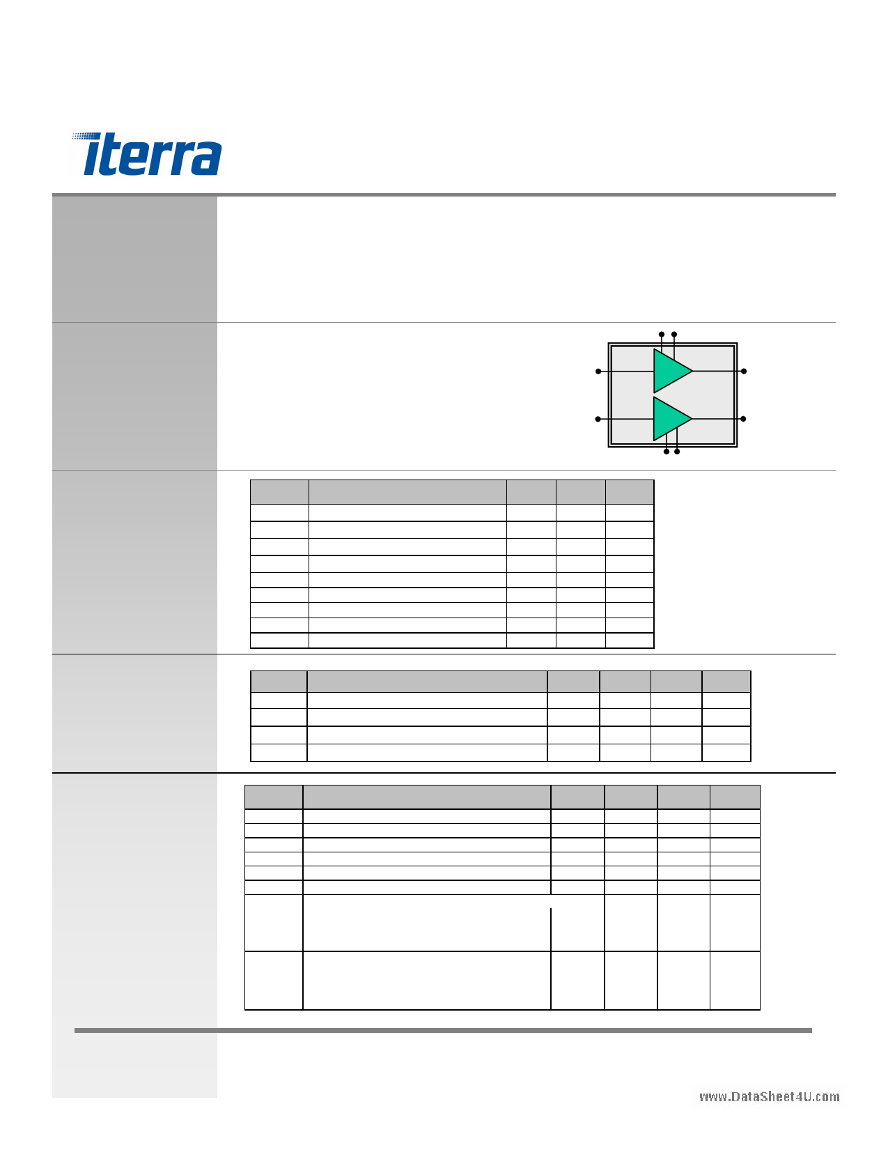
VGG1
IN1
VDD1
CHANNEL 1
OUT1
IN2
VGG2
CHANNEL 2
VDD2
OUT2
Min. Max. Units
11 V
-2 0 V
800 mA
1.6 mA
27 dBm
5W
150 °C
320 °C
-65 150 °C
Symbol
Tb
V D D 1, 2
V GG1, 2
IDQ1,2
Parameters/conditions
Operating temperature range (backside)
Positive bias supply
Negative bias supply
DC supply drain current
Min.
-40
-0.4
Typ.
-0.6
300
Max.
85
9
-0.9
400
Units
oC
V
V
mA
Symbol
BW
S21
S11
S22
S12
Ps at
P1dB
Parameters/conditions
Frequency range
Small signal gain
Gain flatness
Input return loss
Output return loss
Is olation
Saturated output power at 3-dB gain compression
2 - 10 GHz
2 - 20 GHz
2 - 26.5 GHz
Output power at 1-dB gain compression
2 - 10 GHz
2 - 20 GHz
2 - 26.5 GHz
Min.
2
7
8
8
30
27.5
26.5
23
27
26
22.5
Typ.
10
+/-1
10
10
29.5
28.5
25
29
28
24.5
Max.
26.5
Units
GHz
dB
dB
dB
dB
dB
dBm
dBm
dBm
dBm
dBm
dBm
www.iterrac.com
This is Preliminary data sheet. See “Product Status Definitions”
on Web site or catalog for product development status.
December 27, 2006 Doc. 1324 Rev. 1.0
1
iTerra Communications
2400 Geng Road, Ste. 100, Palo Alto, CA 94303
Phone (650) 424-1937, Fax (650) 424-1938
1 page 
iT2002
2 to 26.5 GHz
Dual-Channel, High-Power Amplifier
(Preliminary Information)
Recommended
Procedure
for Biasing and
Operation
www.DataSheet4U.com
CAUTION: LOSS OF GATE VOLTAGE (Vgg1,2) WHILE CORRESPONDING DRAIN VOLTAGE
(Vdd1,2) IS PRESENT CAN DAMAGE THE AMPLIFIER.
The following procedure must be considered to properly test the amplifier.
The iT2002 amplifier is biased with a positive drain supply (VDD1,2 per channel) and one negative gate
supply (VGG1,2 per channel) (Channel 1 and Channel 2). The recommended bias condition for the
iT2002 is VDD1,2= 9.0 V, IDQ1,2 = 300 mA. To achieve this drain current level, VGG1,2 is typically
biased between –0.7 V and –0.9 V. The gate voltage (VGG1/2) MUST be applied prior to the drain
voltage (VDD1,2) during power up and removed after the drain voltage is removed during the power
down. Drain bias VDD1,2 can be applied to the drain (P5-P6). Alternatively, the positive power
supply can be applied through an external bias tee to the RF output pad (P3-P4) .
Application
Information
CAUTION: THIS IS AN ESD SENSITIVE DEVICE
Chip carrier material should be selected to have GaAs-compatible thermal coefficient of expansion
and high thermal conductivity such as copper molybdenum or copper tungsten. The chip carrier
should be machined, finished flat, plated with gold over nickel, and be capable of withstanding
325°C for 15 min.
Die attachment for power devices should utilize gold/tin (80/20) eutectic alloy solder and should
avoid a hydrogen environment for PHEMT devices. Note that the backside of the chip is gold
plated and is used as RF and DC ground.
These GaAs devices should be handled with care and stored in dry nitrogen environment to
prevent contamination of bonding surfaces. These are ESD-sensitive devices and should be
handled with caution, including the use of wrist-grounding straps. All die attach and wire/ribbon
bond equipment must be well grounded to prevent static discharges through the device.
Recommended wire bonding uses gold ribbon 3 mil wide and 0.5 mil thick as short as practical
allowing for appropriate stress relief. The RF input and output bonds should be typically 12 mil long
corresponding to a typical 2 mil gap between the chip and the substrate material.
Eutectic Die
Attachment
iTerra recommends 80/20 AuSn preforms be used for eutectic attachment of its high-power
GaAs die. Die attachment should be performed under forming gas or dry nitrogen. All passive
components should be attached prior to mounting the GaAs die. Place the chip carrier or
package on a heated stage that has a temperature of 290o C controlled to +/- 5o C, with a
maximum temperature of less than 300o C. Before and after placing the die on the 290o C
heated stage, the die should be placed on a 150o C heated stage to minimize thermal shock.
This is essential for die with dimensions greater than 1 mm. Place the AuSn preform on the
carrier or package and let it melt. Using tweezers, pick up the GaAs die and scrub it several
times for 5 to 15 s. After the die is positioned, remove the carrier or substrate from the heated
stage. Maximum dwell time is 1 min., and typically 30 s or less.
www.iterrac.com
This is Preliminary data sheet. See “Product Status Definitions”
on Web site or catalog for product development status.
December 27, 2006 Doc. 1324 Rev. 1.0
5
iTerra Communications
2400 Geng Road, Ste. 100, Palo Alto, CA 94303
Phone (650) 424-1937, Fax (650) 424-1938
5 Page | ||
| Páginas | Total 5 Páginas | |
| PDF Descargar | [ Datasheet iT2002.PDF ] | |
Hoja de datos destacado
| Número de pieza | Descripción | Fabricantes |
| iT2001P | 1 to 20 GHz medium gain high-power amplifier | Iterra |
| iT2002 | 2 to 26.5 GHz dual-channel high-power amplifier | Iterra |
| iT2005 | Power Amplifier | gigoptix |
| iT2005F | Power Amplifier | gigoptix |
| Número de pieza | Descripción | Fabricantes |
| SLA6805M | High Voltage 3 phase Motor Driver IC. |
Sanken |
| SDC1742 | 12- and 14-Bit Hybrid Synchro / Resolver-to-Digital Converters. |
Analog Devices |
|
DataSheet.es es una pagina web que funciona como un repositorio de manuales o hoja de datos de muchos de los productos más populares, |
| DataSheet.es | 2020 | Privacy Policy | Contacto | Buscar |