|
|
|
PDF PIC17C752 Data sheet ( Hoja de datos )
| Número de pieza | PIC17C752 | |
| Descripción | High-Performance 8-Bit CMOS EPROM Microcontrollers | |
| Fabricantes | Microchip Technology | |
| Logotipo | ||
1. PIC17C752 Hay una vista previa y un enlace de descarga de PIC17C752 (archivo pdf) en la parte inferior de esta página. Total 70 Páginas | ||
|
No Preview Available !
www.DataSheet4U.com
PIC17C75X
High-Performance 8-Bit CMOS EPROM Microcontrollers
Devices included in this data sheet:
• PIC17C752
• PIC17C756
Microcontroller Core Features:
• Only 58 single word instructions to learn
• All single cycle instructions (121 ns) except for
program branches and table reads/writes which
are two-cycle
• Operating speed:
B - DC - 33 MHz clock input
- DC - 121 ns instruction cycle
Device
Memory
Program (x16)
Data (x8)
PIC17C752
8K
454
PIC17C756
16K
B • Hardware Multiplier
902
• Interrupt capability
• 16 level deep hardware stack
• Direct, indirect, and relative addressing modes
• Internal/external program memory execution
• Capable of addressing 64K x 16 program memory
space
Peripheral Features:
• 50 I/O pins with individual direction control
• High current sink/source for direct LED drive
- RA2 and RA3 are open drain, high voltage
(12V), high current (60 mA), I/O pins
• Four capture input pins
- Captures are 16-bit, max resolution 121 ns
• Three PWM outputs
- PWM resolution is 1- to 10-bits
• TMR0: 16-bit timer/counter with
8-bit programmable prescaler
• TMR1: 8-bit timer/counter
• TMR2: 8-bit timer/counter
• TMR3: 16-bit timer/counter
• Two Universal Synchronous Asynchronous
Receiver Transmitters (USART/SCI)
- Independant baud rate generators
• 10-bit, 12 channel analog-to-digital converter
• Synchronous Serial Port (SSP) with SPI™ and
I2C™ modes (including I2C master mode)
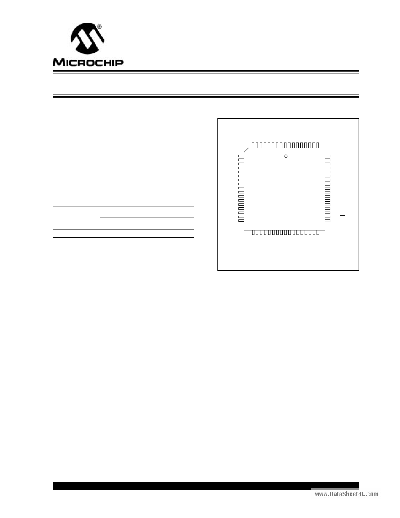
Pin Diagrams
LCC
RD1/AD9
RD0/AD8
RE0/ALE
RE1/OE
RE2/WR
RE3/CAP4
MCLR/VPP
TEST
NC
VSS
VDD
RF7/AN11
RF6/AN10
RF5/AN9
RF4/AN8
RF3/AN7
RF2/AN6
10
11
12
13
14
15
16
17
18
19
20
21
22
23
24
25
26
PIC17C75X
Top View
60 RA0/INT
59 RB0/CAP1
58 RB1/CAP2
57 RB3/PWM2
56 RB4/TCLK12
55 RB5/TCLK3
54 RB2/PWM1
53 VSS
52 NC
51 OSC2/CLKOUT
50 OSC1/CLKIN
49 VDD
48 RB7/SDO
47 RB6/SCK
46 RA3/SDI/SDA
45 RA2/SS/SCL
44 RA1/T0CKI
Special Microcontroller Features:
• Power-on Reset (POR), Power-up Timer (PWRT)
and Oscillator Start-up Timer (OST)
• Watchdog Timer (WDT) with its own on-chip RC
oscillator for reliable operation
• Brown-out Reset
• Code-protection
• Power saving SLEEP mode
• Selectable oscillator options
CMOS Technology:
• Low-power, high-speed CMOS EPROM
technology
• Fully static design
• Wide operating voltage range (2.5V to 6.0V)
• Commercial and Industrial temperature ranges
• Low-power consumption
- < 5 mA @ 5V, 4 MHz
- 100 µA typical @ 4.5V, 32 kHz
- < 1 µA typical standby current @ 5V
© 1997 Microchip Technology Inc.
Preliminary
DS30264A-page 1
1 page 
www.DataSheet4U.com
1.0 OVERVIEW
This data sheet covers the PIC17C75X group of the
PIC17CXXX family of microcontrollers. The following
devices are discussed in this data sheet:
• PIC17C752
• PIC17C756
The PIC17C75X devices are 68-Pin, EPROM-based
members of the versatile PIC17CXXX family of
low-cost, high-performance, CMOS, fully-static, 8-bit
microcontrollers.
All PIC16/17 microcontrollers employ an advanced
RISC architecture. The PIC17CXXX has enhanced
core features, 16-level deep stack, and multiple internal
and external interrupt sources. The separate instruc-
tion and data buses of the Harvard architecture allow a
16-bit wide instruction word with a separate 8-bit wide
data path. The two stage instruction pipeline allows all
instructions to execute in a single cycle, except for pro-
gram branches (which require two cycles). A total of 58
instructions (reduced instruction set) are available.
Additionally, a large register set gives some of the
architectural innovations used to achieve a very high
performance. For mathematical intensive applications
all devices have a single cycle 8 x 8 Hardware Multi-
plier.
PIC17CXXX microcontrollers typically achieve a 2:1
code compression and a 4:1 speed improvement over
other 8-bit microcontrollers in their class.
PIC17C75X devices have up to 902 bytes of RAM and
50 I/O pins. In addition, the PIC17C75X adds several
peripheral features useful in many high performance
applications including:
• Four timer/counters
• Four capture inputs
• Three PWM outputs
• Two independant Universal Synchronous Asyn-
chronous Receiver Transmitters (USARTs)
• An A/D converter (12 channel, 10-bit resolution)
• A Synchronous Serial Port
(SPI and I2C w/ Master mode)
These special features reduce external components,
thus reducing cost, enhancing system reliability and
reducing power consumption.
There are four oscillator options, of which the single pin
RC oscillator provides a low-cost solution, the LF oscil-
lator is for low frequency crystals and minimizes power
consumption, XT is a standard crystal, and the EC is for
external clock input.
The SLEEP (power-down) mode offers additional
power saving. Wake-up from SLEEP can occur through
several external and internal interrupts and device
resets.
A highly reliable Watchdog Timer with its own on-chip
RC oscillator provides protection against software mal-
function.
PIC17C75X
There are four configuration options for the device
operational mode:
• Microprocessor
• Microcontroller
• Extended microcontroller
• Protected microcontroller
The microprocessor and extended microcontroller
modes allow up to 64K-words of external program
memory.
Brown-out Reset circuitry has also been added to the
device. This allows a device reset to occur if the device
VDD falls below the Brown-out voltage trip point
(BVDD). The chip will remain in Brown-out Reset until
VDD rises above BVDD.
Table 1-1 lists the features of the PIC17CXXX devices.
A UV-erasable CERQUAD-packaged version (compat-
ible with PLCC) is ideal for code development while the
cost-effective One-Time Programmable (OTP) version
is suitable for production in any volume.
The PIC17C75X fits perfectly in applications that
require extremely fast execution of complex software
programs. These include applications ranging from
precise motor control and industrial process control to
automotive, instrumentation, and telecom applications.
The EPROM technology makes customization of appli-
cation programs (with unique security codes, combina-
tions, model numbers, parameter storage, etc.) fast
and convenient. Small footprint package options
(including die sales) make the PIC17C75X ideal for
applications with space limitations that require high
performance.
An In-circuit Serial Programming (ISP) feature allows:
• Flexibility of programming the software code as
one of the last steps of the manufacturing process
High speed execution, powerful peripheral features,
flexible I/O, and low power consumption all at low cost
make the PIC17C75X ideal for a wide range of embed-
ded control applications.
1.1 Family and Upward Compatibility
The PIC17CXXX family of microcontrollers have archi-
tectural enhancements over the PIC16C5X and
PIC16CXX families. These enhancements allow the
device to be more efficient in software and hardware
requirements. Refer to Appendix A for a detailed list of
enhancements and modifications. Code written for
PIC16C5X or PIC16CXX can be easily ported to
PIC17CXXX devices (Appendix B).
1.2 Development Support
The PIC17CXXX family is supported by a full-featured
macro assembler, a software simulator, an in-circuit
emulator, a universal programmer, a “C” compiler, and
fuzzy logic support tools. For additional information see
Section 19.0.
© 1997 Microchip Technology Inc.
Preliminary
DS30264A-page 5
5 Page 
www.DataSheet4U.com
PIC17C75X
TABLE 3-1: PINOUT DESCRIPTIONS
Name
DIP
No.
PLCC
No.
TQFP
No.
I/O/P
Type
Buffer
Type
Description
OSC1/CLKIN
47 50 39 I ST Oscillator input in crystal/resonator or RC oscillator mode.
External clock input in external clock mode.
OSC2/CLKOUT 48 51 40 O — Oscillator output. Connects to crystal or resonator in crystal
oscillator mode. In RC oscillator or external clock modes
OSC2 pin outputs CLKOUT which has one fourth the fre-
quency (FOSC/4) of OSC1 and denotes the instruction cycle
rate.
MCLR/VPP
15 16
7 I/P ST Master clear (reset) input or Programming Voltage (VPP)
input. This is the active low reset input to the chip.
PORTA is a bi-directional I/O Port except for RA0 and RA1
which are input only.
RA0/INT
56 60 48 I ST
RA0 can also be selected as an external interrupt
input. Interrupt can be configured to be on positive or
negative edge.
RA1/T0CKI
41 44 33 I ST
RA1 can also be selected as an external interrupt
input, and the interrupt can be configured to be on pos-
itive or negative edge. RA1 can also be selected to be
the clock input to the Timer0 timer/counter.
RA2/SS/SCL
42 45 34 I/O ST
RA2 can also be used as the slave select input for the
SPI or the clock input for the I2C bus.
High voltage, high current, open drain input/output port
pin.
RA3/SDI/SDA
43 46 35 I/O ST
RA3 can also be used as the data input for the SPI or
the data for the I2C bus.
High voltage, high current, open drain input/output port
pin.
RA4/RX1/DT1
40 43 32 I/O † ST
RA4 can also be selected as the USART1 (SCI) Asyn-
chronous Receive or USART1 (SCI) Synchronous
Data.
RA5/TX1/CK1
39 42 31 I/O † ST
RA5 can also be selected as the USART1 (SCI) Asyn-
chronous Transmit or USART1 (SCI) Synchronous
Clock.
PORTB is a bi-directional I/O Port with software config-
urable weak pull-ups.
RB0/CAP1
55 59 47 I/O ST
RB0 can also be the Capture1 input pin.
RB1/CAP2
54 58 46 I/O ST
RB1 can also be the Capture2 input pin.
RB2/PWM1
50 54 42 I/O ST
RB2 can also be the PWM1 output pin.
RB3/PWM2
53 57 45 I/O ST
RB3 can also be the PWM2 output pin.
RB4/TCLK12
52 56 44 I/O ST
RB4 can also be the external clock input to Timer1 and
Timer2.
RB5/TCLK3
51 55 43 I/O ST
RB5 can also be the external clock input to Timer3.
RB6/SCK
44 47 36 I/O ST
RB6 can also be used as the master/slave clock for the
SPI.
RB7/SDO
45 48 37 I/O ST
RB7 can also be used as the data output for the SPI.
Legend: I = Input only; O = Output only; I/O = Input/Output; P = Power; — = Not Used; TTL = TTL input;
ST = Schmitt Trigger input.
† The output is only available by the Peripheral operation.
© 1997 Microchip Technology Inc.
Preliminary
DS30264A-page 11
11 Page | ||
| Páginas | Total 70 Páginas | |
| PDF Descargar | [ Datasheet PIC17C752.PDF ] | |
Hoja de datos destacado
| Número de pieza | Descripción | Fabricantes |
| PIC17C752 | High-Performance 8-bit CMOS EPROM Microcontrollers | Microchip Technology |
| PIC17C752 | High-Performance 8-Bit CMOS EPROM Microcontrollers | Microchip Technology |
| PIC17C756 | High-Performance 8-Bit CMOS EPROM Microcontrollers | Microchip Technology |
| PIC17C756A | High-Performance 8-bit CMOS EPROM Microcontrollers | Microchip Technology |
| Número de pieza | Descripción | Fabricantes |
| SLA6805M | High Voltage 3 phase Motor Driver IC. |
Sanken |
| SDC1742 | 12- and 14-Bit Hybrid Synchro / Resolver-to-Digital Converters. |
Analog Devices |
|
DataSheet.es es una pagina web que funciona como un repositorio de manuales o hoja de datos de muchos de los productos más populares, |
| DataSheet.es | 2020 | Privacy Policy | Contacto | Buscar |