|
|
|
PDF K3563 Data sheet ( Hoja de datos )
| Número de pieza | K3563 | |
| Descripción | MOSFET ( Transistor ) - 2SK3563 | |
| Fabricantes | Toshiba Semiconductor | |
| Logotipo | ||
 1. - 500V, 5A, MOSFET, 2SK3563 Hay una vista previa y un enlace de descarga de K3563 (archivo pdf) en la parte inferior de esta página. Total 3 Páginas | ||
|
No Preview Available !
www.DataSheet4U.com
TENTATIVE
2SK3563
TOSHIBA Field Effect Transistor Silicon N Channel MOS Type (π-MOSⅥ)
2SK3563
Switching Regulator Applications
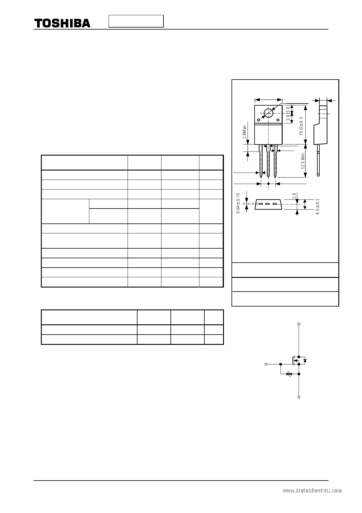
unit:mm
• Low drain-source ON resistance: RDS (ON) = 1.35Ω (typ.)
• High forward transfer admittance: |Yfs| = 3.5S (typ.)
• Low leakage current: IDSS = 100 μA (VDS = 500 V)
• Enhancement-mode: Vth = 2.0~4.0 V (VDS = 10 V, ID = 1 mA)
10±0.3
φ3.2±0.2
2.7±0.2
Maximum Ratings (Ta = 25°C)
Characteristics
Drain-source voltage
Drain-gate voltage (RGS = 20 kΩ)
Gate-source voltage
Drain current
DC (Note 1)
Pulse (t = 1 ms)
(Note 1)
Drain power dissipation (Tc = 25°C)
Single pulse avalanche energy
(Note 2)
Avalanche current
Repetitive avalanche energy (Note 3)
Channel temperature
Storage temperature range
Symbol
VDSS
VDGR
VGSS
ID
IDP
PD
EAS
IAR
EAR
Tch
Tstg
Thermal Characteristics
Rating
500
500
±30
5
20
35
180
5
3.5
150
-55~150
Unit
V
V
V
A
W
mJ
A
mJ
°C
°C
1.1
1.1
0.69±0.15
2.54±0.25
2.54±0.25
123
1. Gate
2. Drain
3. Source
JEDEC
JEITA
TOSHIBA
―
―
―
Characteristics
Symbol
Max Unit
Thermal resistance, channel to case
Thermal resistance, channel to ambient
Rth (ch-c)
Rth (ch-a)
3.57 °C/W
62.5 °C/W
Note 1: Please use devices on conditions that the channel temperature is below 150°C.
Note 2: VDD = 90 V, Tch = 25°C(initial), L = 12.2 mH, IAR = 5 A, RG = 25 Ω
1
Note 3: Repetitive rating: Pulse width limited by maximum channel temperature
This transistor is an electrostatic sensitive device. Please handle with caution.
2
3
1 2003-01-27
1 page | ||
| Páginas | Total 3 Páginas | |
| PDF Descargar | [ Datasheet K3563.PDF ] | |
Hoja de datos destacado
| Número de pieza | Descripción | Fabricantes |
| K3561 | MOSFET ( Transistor ) - 2SK3561 | Toshiba Semiconductor |
| K3562 | MOSFET ( Transistor ) - 2SK3562 | Toshiba Semiconductor |
| K3562M | IF Filter | EPCOS |
| K3563 | MOSFET ( Transistor ) - 2SK3563 | Toshiba Semiconductor |
| Número de pieza | Descripción | Fabricantes |
| SLA6805M | High Voltage 3 phase Motor Driver IC. |
Sanken |
| SDC1742 | 12- and 14-Bit Hybrid Synchro / Resolver-to-Digital Converters. |
Analog Devices |
|
DataSheet.es es una pagina web que funciona como un repositorio de manuales o hoja de datos de muchos de los productos más populares, |
| DataSheet.es | 2020 | Privacy Policy | Contacto | Buscar |