|
|
|
PDF A8483 Data sheet ( Hoja de datos )
| Número de pieza | A8483 | |
| Descripción | Step-up Converter | |
| Fabricantes | Allegro MicroSystems | |
| Logotipo | ||
Hay una vista previa y un enlace de descarga de A8483 (archivo pdf) en la parte inferior de esta página. Total 9 Páginas | ||
|
No Preview Available !
www.DataSheet4U.com
Package EK:
MLP/TDFN, 3 × 3 mm
0.75 mm Nominal Height
A8483
1.2 MHz Step-up Converter
for Display Bias Supply
Approximate Scale 1:1
FEATURES
Output voltage up to 35 V
2.5 to 10 V input
0.9 to 18 V input with separate bias supply
Delivers 15 V at 15 mA with 2.7 V input
Constant 1.2 MHz switching frequency provides low noise
350 mA switch current limit
1 μA shutdown current
Low-noise PWM/analog dimming
L1
5 10 µH 1
VIN SW
VSUPPLY C1
1 µF
Li-ion
2.5 V to
5.5 V
A8483
EN GND FB
423
Enable
VOUT
D1
R1
820 kΩ
R2
39 kΩ
C2
1 µF
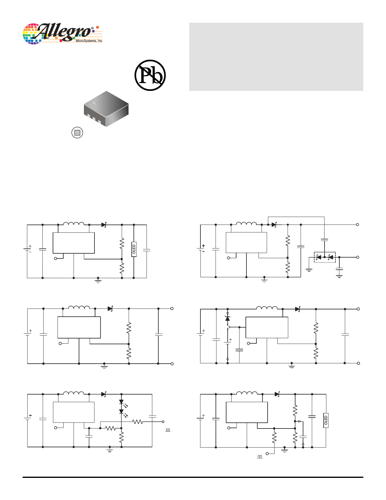
Figure 1. OLED Bias Supply. Use for cell phones, MP3
players, DSCs, and PDAs.
L1
5 10 µH 1
VIN SW
VOUT
D1
32 V, 18 mA
25 V, 25 mA
VSUPPLY C1
1 µF
5V
A8483
EN GND FB
423
R1
768 kΩ for
VOUT = 32 V
604 kΩ for
VOUT = 25 V
C2
1 µF / 50 V
Enable
R2
15 kΩ
The A8483 is a current mode step-up dc-to-dc converter,
available in a 5-pin 3 mm × 3 mm thermally enhanced
MLP/TDFN lead (Pb) free package. Smaller external
components and integrated 36 V switch reduce component
count and footprint for a variety of applications.
APPLICATIONS
OLED bias supply / WLED backlight
Portable battery-powered equipment
Cellular phones
PDAs (Personal Digital Assistant)
Camcorders, personal stereos, MP3 players, cameras
Mobile GPS systems
L1
5 10 µH 1
VIN SW
VSUPPLY C1
1 µF
Li-ion
2.5 V to
5.5 V
A8483
EN GND FB
423
Enable
D1
R1
732 kΩ
R2
39 kΩ
C2
0.47 µF
IOUT1 + IOUT2 = 15 mA
VOUT1
+12 V
C3
0.47 µF
VOUT2
D2 –12 V
C4
0.47 µF
Figure 2. Small LCD Bias Supply. Li+ battery to ±12 V.
Connect either VZ or VBIAS
VZ
7.5 V
L1
22 µH
1
SW
VSUPPLY
12 V
C1
1 µF
VBIAS
VIN
5
A8483
EN GND FB
423
5 V Enable
C3
0.1 µF
VOUT
D1
32 V, 40 mA
25 V, 80 mA
R1
768 kΩ for
VOUT = 32 V
604 kΩ for
VOUT = 25 V
C2
1 µF / 50 V
R2
15 kΩ
Figure 3. LCD TV, Plasma TV Bias, FED Display,
Varactor Diode Bias. Using 5 V input.
L1
5
10 µH
1
VIN SW
VSUPPLY C1
1 µF
Li-ion
2.5 V to
5.5 V
A8483
EN GND FB
423
Enable
Cf
0.01 µF
VOUT
D1
R3
24 kΩ
R2
5 kΩ
R1
47 Ω
C2
0.22 µF
VC
Analog Voltage or
PWM
Figure 5. WLED Backlighting.
A8483-DS, Rev. 1
Figure 4. LCD TV, Plasma TV Bias, FED Display,
Varactor Diode Bias. Using 12 V input.
VSUPPLY
Li-ion
2.5 V to
5.5 V
C1
1 µF
L1
5 10 µH 1
VIN SW
A8483
EN GND FB
423
Enable
R3
160 kΩ
VOUT
D1
R1
560 kΩ
R2
47 kΩ
C2
1 µF
Cf
1 nF
Analog Voltage or
Cf for PWM dimming only
PWM 10 kHz
VC
Figure 6. OLED Bias Supply. Use for low-noise PWM
dimming, or with analog voltage through the FB pin.
1 page 
A8483 1.2 MHz Step-up Converter for Display Bias Supply
Applications Information
Dimming Control
Display dimming can be achieved by controlling the output
voltage, VOUT , using the FB pin. The circuitry behind the FB
pin is flexible, to accommodate a variety of schemes used for
dimming:
• Adjust the duty cycle of the pulse train applied to the FB pin
through resistor R3, as shown in figure 11. Capacitor Cf is
used to generate the average voltage level. Variation of output
voltage with PWM duty cycle is shown in figure 9.
• Apply a constant dc voltage to the FB pin through resistor
R3, as shown in figure 12. Variation of output voltage with dc
voltage are shown in figure 10.
• Selection of the resistor connected between the FB pin and
GND, as shown in figure 12 for OLED applications, and in
figure 13 for WLED applications. The voltage drop across
the transistor should be negligible compared to the FB sense
voltage.
17
15
13
11
9
7
5
3
10 20 30 40 50 60 70 80 90
Duty Cycle (%)
Figure 9. PWM Dimming Control of Duty Cycle. Performance of 5 V input
circuit shown in figure 3.
20
18
16
14
12
10
8
6
4
2
0
0.2 0.4 0.6 0.8
VC (V)
1
Figure 10. DC Voltage Dimming Control of Duty Cycle. Performance of
circuit shown in figure 11.
A8483-DS, Rev. 1
Soft Start
Output voltage rise time at power-on can be extended by using a
soft start circuit, such as the one shown in figure 14 for an OLED
application, and in figure 16 for a WLED application. At power-
on, the device duty cycle begins initially at a high level, drawing
a large current from the input supply, VIN. The soft-start circuits
shown can reduce the level of current flow by controlling the FB
pin.
When a signal is applied to the EN pin, capacitor C3 discharges,
pulling the FB pin high, and reducing VOUT to a minimum.
When the EN signal is removed, C3 recharges and as it does, the
voltage drop across R3 reduces, allowing the device duty cycle to
VSUPPLY
Li-ion
2.5 V to
5.5 V
C1
1 µF
L1
5 10 µH 1
VIN SW
A8483
EN GND FB
423
Enable
R3
160 kΩ
VOUT
D1
R1
560 kΩ
R2
47 kΩ
C2
1 µF
Cf
1 nF
Analog Voltage or
PWM 10 kHz
VC
Cf for PWM dimming only
Figure 11. OLED Bias Supply. Use for low-noise PWM dimming,
or with analog voltage through the FB pin.
L1
5 10 µH 1
VIN SW
VSUPPLY C1
1 µF
Li-ion
2.5 V to
5.5 V
A8483
EN GND FB
423
Enable
R3
47 kΩ
VOUT
D1
R1
560 kΩ
R2
47 kΩ
VC
Q1
C2
10 µF
Cf
1 nF
Figure 12. OLED Dimming Control. Single-bit resolution using
external transistor.
L1
5 10 µH 1
VIN SW
VOUT
D1
VSUPPLY C1
1 µF
Li-ion
2.5 V to
5.5 V
A8483
EN GND FB
423
Enable
R2
80 Ω
VC
R1
80 Ω
Q1
C2
0.22 µF
Figure 13. WLED Dimming Control. Single-bit resolution using
external transistor.
Allegro MicroSystems, Inc.
5
115 Northeast Cutoff, Box 15036
Worcester, Massachusetts 01615-0036 (508) 853-5000
www.allegromicro.com
5 Page | ||
| Páginas | Total 9 Páginas | |
| PDF Descargar | [ Datasheet A8483.PDF ] | |
Hoja de datos destacado
| Número de pieza | Descripción | Fabricantes |
| A8480 | Boost Regulator | Allegro Micro Systems |
| A8483 | Step-up Converter | Allegro MicroSystems |
| Número de pieza | Descripción | Fabricantes |
| SLA6805M | High Voltage 3 phase Motor Driver IC. |
Sanken |
| SDC1742 | 12- and 14-Bit Hybrid Synchro / Resolver-to-Digital Converters. |
Analog Devices |
|
DataSheet.es es una pagina web que funciona como un repositorio de manuales o hoja de datos de muchos de los productos más populares, |
| DataSheet.es | 2020 | Privacy Policy | Contacto | Buscar |