|
|
|
PDF LTC2620 Data sheet ( Hoja de datos )
| Número de pieza | LTC2620 | |
| Descripción | (LTC2600 - LTC2620) 3V/5V Octal 12-bit Rail-to-rail DAC | |
| Fabricantes | Linear Technology | |
| Logotipo | ||
1. LTC2620 Hay una vista previa y un enlace de descarga de LTC2620 (archivo pdf) en la parte inferior de esta página. Total 16 Páginas | ||
|
No Preview Available !
LTC2600/LTC2610/LTC2620
FEATURES
Octal 16-/14-/12-Bit
Rail-to-Rail DACs in 16-Lead SSOP
DESCRIPTIO
s Smallest Pin Compatible Octal DACs:
LTC2600: 16 Bits
LTC2610: 14 Bits
LTC2620: 12 Bits
s Guaranteed 16-Bit Monotonic Over Temperature
s Tiny 16-Lead Narrow SSOP Package
s Wide 2.5V to 5.5V Supply Range
s Low Power Operation: 250µA per DAC at 3V
s Individual Channel Power-Down to 1µA, Max
s Ultralow Crosstalk between DACs (<10µV)
s High Rail-to-Rail Output Drive (±15mA, Min)
s Double-Buffered Digital Inputs
s Pin-Compatible 10-/8-Bit Versions
(LTC1660/LTC1665)
U
APPLICATIO S
s Mobile Communications
www.DataSheet4U.csom Process Control and Industrial Automation
s Instrumentation
s Automatic Test Equipment
The LTC®2600/LTC2610/LTC2620 are octal 16-, 14- and
12-bit, 2.5V-to-5.5V rail-to-rail voltage-output DACs in
16-lead narrow SSOP packages. They have built-in high
performance output buffers and are guaranteed mono-
tonic.
These parts establish new board-density benchmarks for
16- and 14-bit DACs and advance performance standards
for output drive, crosstalk and load regulation in single-
supply, voltage-output multiples.
The parts use a simple SPI/MICROWIRETM compatible
3-wire serial interface which can be operated at clock rates
up to 50MHz. Daisy-chain capability and a hardware CLR
function are included.
The LTC2600/LTC2610/LTC2620 incorporate a power-on
reset circuit. During power-up, the voltage outputs rise
less than 10mV above zero scale; and after power-up, they
stay at zero scale until a valid write and update take place.
, LTC and LT are registered trademarks of Linear Technology Corporation.
MICROWIRE is a trademark of National Semiconductor Corporation.
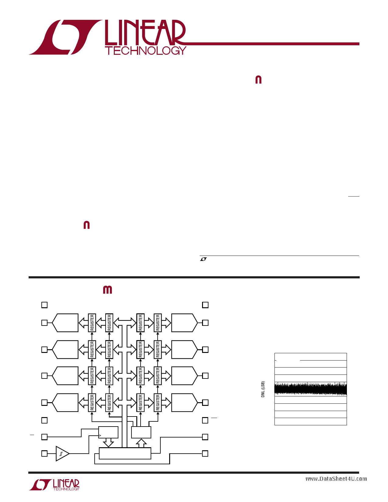
BLOCK DIAGRA
GND 1
VOUT A 2
DAC A
DAC H
16 VCC
15 VOUT H
VOUT B 3
DAC B
VOUT C 4
DAC C
VOUT D 5
REF 6
CS/LD 7
SCK 8
DAC D
CONTROL
LOGIC
DECODE
32-BIT SHIFT REGISTER
DAC G
14 VOUT G
DAC F
13 VOUT F
DAC E
12 VOUT E
11 CLR
10 SDO
9 SDI
2600 BD
Differential Nonlinearity (LTC2600)
1.0
VCC = 5V
0.8 VREF = 4.096V
0.6
0.4
0.2
0
–0.2
–0.4
–0.6
–0.8
–1.0
0
16384
32768
CODE
49152 65535
2600 G21
2600f
1
1 page 
LTC2600/LTC2610/LTC2620
TYPICAL PERFOR A CE CHARACTERISTICS
LTC2600/LTC2610/LTC2620
Zero-Scale Error vs Temperature
3
2.5
2.0
1.5
1.0
0.5
0
–50 –30 –10 10 30 50
TEMPERATURE (°C)
70 90
2600 G04
Gain Error vs Temperature
0.4
0.3
0.2
0.1
0
–0.1
–0.2
–0.3
–0.4
–50 –30 –10 10 30 50
TEMPERATURE (°C)
70 90
2600 G05
Offset Error vs VCC
3
2
1
0
–1
–2
–3
2.5 3 3.5 4 4.5 5 5.5
VCC (V)
2600 G06
Gain Error vs VCC
0.4
0.3
0.2
www.DataSheet4U.com 0.1
0
–0.1
–0.2
–0.3
–0.4
2.5 3 3.5 4 4.5
VCC (V)
5 5.5
2600 G07
Midscale Glitch Impulse
VOUT
10mV/DIV
CS/LD
5V/DIV
12nV-s TYP
2.5µs/DIV
2600 G10
ICC Shutdown vs VCC
450
400
350
300
250
200
150
100
50
0
2.5 3 3.5 4 4.5
VCC (V)
5 5.5
2600 G08
Large-Signal Settling
VOUT
0.5V/DIV
VREF = VCC = 5V
1/4-SCALE TO 3/4-SCALE
2.5µs/DIV
2600 G09
Power-On Reset Glitch
VCC
1V/DIV
VOUT
10mV/DIV
44mmVVPPEEAAKK
250µs/DIV
2600 G11
Headroom at Rails vs Output
Current
5.0
4.5 5V SOURCING
4.0
3.5
3V SOURCING
3.0
2.5
2.0
1.5
5V SINKING
1.0
3V SINKING
0.5
0
0 1 2 3 4 5 6 7 8 9 10
IOUT (mA)
2600 G12
2600f
5
5 Page 
U
OPERATIO
INPUT WORD (LTC2600)
COMMAND
ADDRESS
LTC2600/LTC2610/LTC2620
DATA (16 BITS)
C3 C2 C1 C0 A3 A2 A1 A0 D15 D14 D13 D12 D11 D10 D9 D8 D7 D6 D5 D4 D3 D2 D1 D0
MSB
LSB
2600 TBL01
INPUT WORD (LTC2610)
COMMAND
ADDRESS
DATA (14 BITS + 2 DON’T-CARE BITS)
C3 C2 C1 C0 A3 A2 A1 A0 D13 D12 D11 D10 D9 D8 D7 D6 D5 D4 D3 D2 D1 D0 X X
MSB
LSB
2600 TBL02
INPUT WORD (LTC2620)
COMMAND
ADDRESS
DATA (12 BITS + 4 DON’T-CARE BITS)
C3 C2 C1 C0 A3 A2 A1 A0 D11 D10 D9 D8 D7 D6 D5 D4 D3 D2 D1 D0 X X X X
MSB
LSB
2600 TBL03
Daisy-Chain Operation
Thewww.DataSheet4U.com serial output of the shift register appears at the SDO
pin. Data transferred to the device from the SDI input is
delayed 32 SCK rising edges before being output at the
next SCK falling edge.
The SDO output can be used to facilitate control of multiple
serial devices from a single 3-wire serial port (i.e., SCK,
SDI and CS/LD). Such a “daisy chain” series is configured
by connecting SDO of each upstream device to SDI of the
next device in the chain. The shift registers of the devices
are thus connected in series, effectively forming a single
input shift register which extends through the entire chain.
Because of this, the devices can be addressed and con-
trolled individually by simply concatenating their input
words; the first instruction addresses the last device in the
chain and so forth. The SCK and CS/LD signals are
common to all devices in the series.
In use, CS/LD is first taken low. Then the concatenated
input data is transferred to the chain, using SDI of the first
device as the data input. When the data transfer is com-
plete, CS/LD is taken high, completing the instruction
sequence for all devices simultaneously. A single device
can be controlled by using the “no operation” command
(1111) for the other devices in the chain.
Power Down Mode
Command 0100b is reserved for the special “power down”
instruction (see Table 1). Any or all DACs may be powered
down by selecting the appropriate DAC address (n). In this
mode, the digital interface stays active while the analog
circuits are disabled. The static power consumption of the
digital interface is leakage current only. The reference
input and analog outputs are set in a high impedance state,
although the DAC feedback resistors are still in place
loading the DAC outputs with 90kΩ to ground. As shown
in Table 1, any or all of the DACs can be powered back up
by executing an update command to the selected DAC
which will power up that DAC and update its output with
the last loaded DAC word.
Voltage Outputs
Each of the 8 rail-to-rail amplifiers contained in these parts
has guaranteed load regulation when sourcing or sinking
up to 15mA at 5V (7.5mA at 3V).
Load regulation is a measure of the amplifier’s ability to
maintain the rated voltage accuracy over a wide range of
load conditions. The measured change in output voltage
per milliampere of forced load current change is ex-
pressed in LSB/mA.
2600f
11
11 Page | ||
| Páginas | Total 16 Páginas | |
| PDF Descargar | [ Datasheet LTC2620.PDF ] | |
Hoja de datos destacado
| Número de pieza | Descripción | Fabricantes |
| LTC2620 | (LTC2600 - LTC2620) 3V/5V Octal 12-bit Rail-to-rail DAC | Linear Technology |
| LTC2621 | (LTC2601 - LTC2621) 12-Bit Rail-to-rail DACs | Linear Technology |
| LTC2622 | (LTC2602 - LTC2622) Rail-to-rail DACs | Linear Technology |
| LTC2624 | (LTC2604 - LTC2624) Rail-to-rail Voltage Output DACs | Linear Technology |
| Número de pieza | Descripción | Fabricantes |
| SLA6805M | High Voltage 3 phase Motor Driver IC. |
Sanken |
| SDC1742 | 12- and 14-Bit Hybrid Synchro / Resolver-to-Digital Converters. |
Analog Devices |
|
DataSheet.es es una pagina web que funciona como un repositorio de manuales o hoja de datos de muchos de los productos más populares, |
| DataSheet.es | 2020 | Privacy Policy | Contacto | Buscar |