|
|
|
PDF FOD3180 Data sheet ( Hoja de datos )
| Número de pieza | FOD3180 | |
| Descripción | High Speed MOSFET Gate Driver Optocoupler | |
| Fabricantes | Fairchild Semiconductor | |
| Logotipo | ||
Hay una vista previa y un enlace de descarga de FOD3180 (archivo pdf) en la parte inferior de esta página. Total 13 Páginas | ||
|
No Preview Available !
www.DataSheet4U.com
January 2007
FOD3180
2A Output Current, High Speed MOSFET Gate Driver
Optocoupler
tm
Features
■ Guaranteed operating temperature range of -40°C to
+100°C
■ 2A minimum peak output current
■ High speed response: 200ns max propagation delay
over temperature range
■ 250kHz maximum switching speed
■ 30ns typ pulse width distortion
■ Wide VCC operating range: 10V to 20V
■ 5000Vrms, 1 minute isolation
■ Under voltage lockout protection (UVLO) with
hysteresis
■ Minimum creepage distance of 7.0mm
■ Minimum clearance distance of 7.0mm
■ C-UL, UL and VDE* safety agency approvals pending
■ RDS(ON) of 1.5Ω (typ.) offers lower power dissipation
■ 10kV/µs minimum common mode rejection
Applications
■ Plasma Display Panel
■ High performance DC/DC convertor
■ High performance switch mode power supply
■ High performance uninterruptible power supply
■ Isolated Power MOSFET gate drive
*Requires ‘V’ ordering option
Description
The FOD3180 is a 2A Output Current, High Speed
MOSFET Gate Drive Optocoupler. It consists of a
aluminium gallium arsenide (AlGaAs) light emitting diode
optically coupled to a CMOS detector with PMOS and
NMOS output power transistors integrated circuit power
stage. It is ideally suited for high frequency driving of
power MOSFETs used in Plasma Display Panels
(PDPs), motor control inverter applications and high
performance DC/DC converters.
The device is packaged in an 8-pin dual in-line housing
compatible with 260°C reflow processes for lead free
solder compliance.
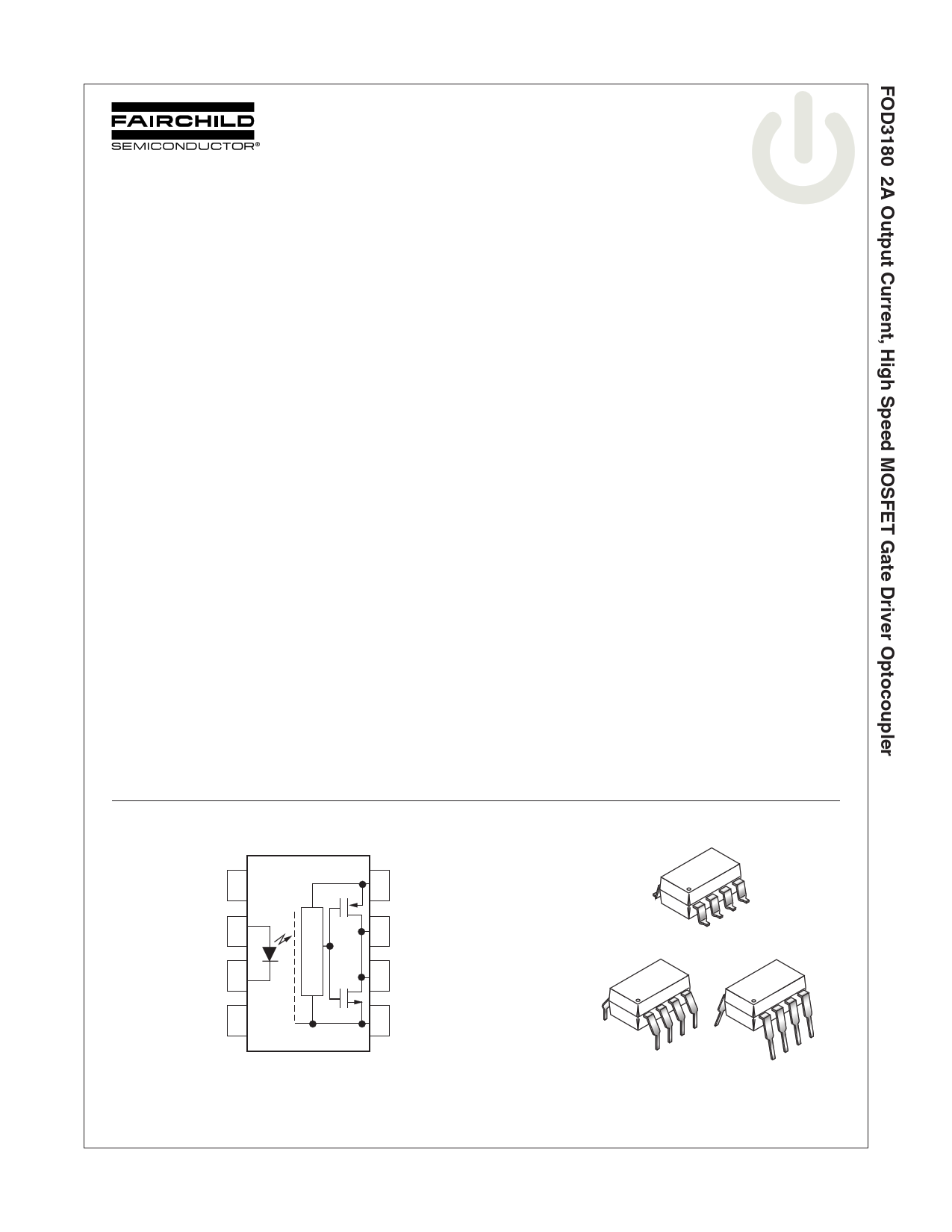
Functional Block Diagram
NO CONNECTION 1
ANODE 2
CATHODE 3
FOD3180
8 VCC
7 OUTPUT
6 OUTPUT
8
1
NO CONNECTION 4
5 VEE
Note:
A 0.1µF bypass capacitor must be connected
between pins 5 and 8.
8
1
8
1
©2005 Fairchild Semiconductor Corporation
FOD3180 Rev. 1.0.3
1
www.fairchildsemi.com
1 page 
Notes:
1. Derate linearly above +70°C free air temperature at a rate of 0.3mA/°C.
2. The output currents IOH and IOL are specified with a capacitive current limited load = (3 x 0.01µF) + 0.5Ω,
frequency = 8kHz, 50% DF. The maximum pulse width of the output current is 300ns, maximum duty cycle = 0.48%.
Output currents specified for different values of VDS for VCC – VEE = 20V with the formula:
VOH = (VCC – VEE) – (IOH x RDS(ON)).
This guarantees operation at IO peak minimum = 2.0A for -40°C to +100°C operating temperature range.
3. The output currents IOH and IOL are specified with a capacitive current limited load = (3 x 0.01µF) + 8.5Ω,
frequency = 8kHz, 50% DF. The maximum pulse width of the output current is 1.5µs, maximum duty cycle = 2.4%.
Output currents specified for different values of VDS for VCC – VEE = 20V with the formula:
VOL = (VCC – VEE) – (IOL x RDS(ON)).
This guarantees operation at IO peak minimum = 0.5A for -40°C to +100°C operating temperature range.
4. Derate linearly above +87°C, free air temperature at the rate of 0.77mW/°C. Refer to Figure 12.
5. No derating required across operating temperature range.
6. In this test, VOH is measured with a dc load current. When driving capacitive load VOH will approach VCC as IOH
approaches zero amps.
7. Maximum pulse width = 1ms, maximum duty cycle = 20%.
8. tPHL propagation delay is measured from the 50% level on the falling edge of the input pulse to the 50% level of the
falling edge of the VO signal. tPLH propagation delay is measured from the 50% level on the rising edge of the input
pulse to the 50% level of the rising edge of the VO signal.
9. PWD is defined as | tPHL – tPLH | for any given device.
10. The difference between tPHL and tPLH between any two FOD3180 parts under same test conditions.
11. Pin 1 and 4 need to be connected to LED common.
12. Common mode transient immunity in the high state is the maximum tolerable dVCM/dt of the common mode pulse
VCM to assure that the output will remain in the high state (i.e. VO > 10.0V).
13. Common mode transient immunity in a low state is the maximum tolerable dVCM/dt of the common mode pulse,
VCM, to assure that the output will remain in a low state (i.e. VO < 1.0V).
14. In accordance with UL 1577, each optocoupler is proof tested by applying an insulation test voltage > 6000Vrms for
1 second (leakage detection current limit II-O < 5µA).
15. Device considered a two-terminal device: pins on input side shorted together and pins on output side shorted
together.
5 www.fairchildsemi.com
FOD3180 Rev. 1.0.3
5 Page 
Reflow Profile
300 245C, 10–30 s
250 260C peak
200
150
100 Time above 183C, <160 sec
50 Ramp up = 2–10C/sec
0
0 0.5 1 1.5 2 2.5 3 3.5 4 4.5
Time (Minute)
• Peak reflow temperature: 260 C (package surface temperature)
• Time of temperature higher than 183 C for 160 seconds or less
• One time soldering reflow is recommended
Output Power Derating
The maximum package power dissipation is 295mW. The pack-
age is limited to this level to ensure that under normal operating
conditions and over extended temperature range that the semi-
conductor junction temperatures do not exceed 125°C. The
package power is composed of three elements; the LED, static
operating power of the output IC, and the power dissipated in
the output power MOSFET transistors. The power rating of the
output IC is 250mW. This power is divided between the static
power of the integrated circuit, which is the product of IDD times
the power supply voltage (VDD – VEE). The maximum IC static
output power is 150mW, (VDD – VEE) = 25V, IDD = 6mA. This
maximum condition is valid over the operational temperature
range of -40°C to +100°C. Under these maximum operating
conditions, the output of the power MOSFET is allowed to dissi-
pate 100mW of power.
The absolute maximum output power dissipation versus ambi-
ent temperature is shown in Figure 12. The output driver is
capable of supplying 100mW of output power over the tempera-
ture range from -40°C to 87°C. The output derates to 90mW at
the absolute maximum operating temperature of 100°C.
Fig. 12 Absolute Maximum Power Dissipation
vs. Ambient Temperature
0.15
VDD – VEE = Max. = 25V
IDD = 6mA
LED Power = 45mW
The output power is the product of the average output current
squared times the output transistor’s RDS(ON):
PO(AVG) = IO(AVG)2 • RDS(ON)
The IO(AVG) is the product of the duty factor times the peak
current flowing in the output. The duty factor is the ratio of the
‘on’ time of the output load current divided by the period of the
operating frequency. An RDS(ON) of 2.0Ω results in an average
output load current of 200mA. The load duty factor is a ratio of
the average output time of the power MOSFET load circuit and
period of the driving frequency.
The maximum permissible, operating frequency is determined
by the load supplied to the output at its resulting output pulse
width. Figure 13 shows an example of a 0.03µF gate to source
capacitance with a series resistance of 8.50Ω. This reactive
load results in a composite average pulse width of 1.5µs. Under
this load condition it is not necessary to derate the absolute
maximum output current until the frequency of operation
exceeds 63kHz.
Fig. 13 Output Current Derating vs. Frequency
2.5
2
1.5
TA = -40°C to 100°C
0.1 Load = .03µF +8.5Ω
VDD = 20V
1 IF = 12mA
LED Duty Factor = 50%
Output Pulse Width = 1.5µs
0.05 0.5
0
1 10 100
0
-40 -20
0
20 40 60 80 100
F – Frequency (kHz)
TA – Ambient Temperature (°C)
11 www.fairchildsemi.com
FOD3180 Rev. 1.0.3
11 Page | ||
| Páginas | Total 13 Páginas | |
| PDF Descargar | [ Datasheet FOD3180.PDF ] | |
Hoja de datos destacado
| Número de pieza | Descripción | Fabricantes |
| FOD3180 | High Speed MOSFET Gate Driver Optocoupler | Fairchild Semiconductor |
| FOD3181 | High Speed MOSFET Gate Driver Optocoupler | Fairchild Semiconductor |
| Número de pieza | Descripción | Fabricantes |
| SLA6805M | High Voltage 3 phase Motor Driver IC. |
Sanken |
| SDC1742 | 12- and 14-Bit Hybrid Synchro / Resolver-to-Digital Converters. |
Analog Devices |
|
DataSheet.es es una pagina web que funciona como un repositorio de manuales o hoja de datos de muchos de los productos más populares, |
| DataSheet.es | 2020 | Privacy Policy | Contacto | Buscar |