|
|
|
PDF 74HC74 Data sheet ( Hoja de datos )
| Número de pieza | 74HC74 | |
| Descripción | Dual D Flip-Flop | |
| Fabricantes | ON Semiconductor | |
| Logotipo | ||
1. 74HC74 Hay una vista previa y un enlace de descarga de 74HC74 (archivo pdf) en la parte inferior de esta página. Total 8 Páginas | ||
|
No Preview Available !
www.DataSheet4U.com
74HC74
Dual D Flip−Flop with Set
and Reset
High−Performance Silicon−Gate CMOS
The 74HC74 is identical in pinout to the LS74. The device inputs are
compatible with standard CMOS outputs; with pullup resistors, they
are compatible with LSTTL outputs.
This device consists of two D flip−flops with individual Set, Reset,
and Clock inputs. Information at a D−input is transferred to the
corresponding Q output on the next positive going edge of the clock
input. Both Q and Q outputs are available from each flip−flop. The Set
and Reset inputs are asynchronous.
Features
• Output Drive Capability: 10 LSTTL Loads
• Outputs Directly Interface to CMOS, NMOS, and TTL
• Operating Voltage Range: 2.0 to 6.0 V
• Low Input Current: 1.0 mA
• High Noise Immunity Characteristic of CMOS Devices
• In Compliance with the JEDEC Standard No. 7A Requirements
• ESD Performance: HBM > 2000 V; Machine Model > 200 V
• Chip Complexity: 128 FETs or 32 Equivalent Gates
• Pb−Free Packages are Available
http://onsemi.com
MARKING
DIAGRAMS
14
1
14
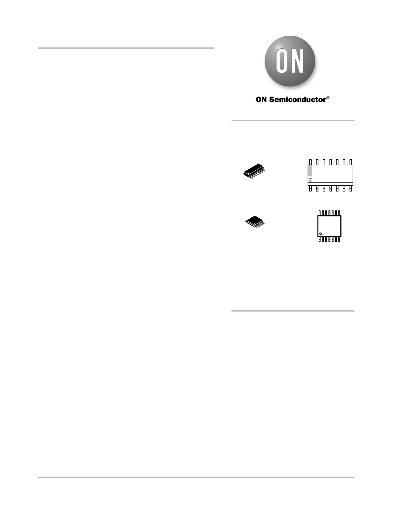
SOIC−14
D SUFFIX
CASE 751A
1
HC74G
AWLYWW
14
1
TSSOP−14
DT SUFFIX
CASE 948G
14
HC
74
ALYW G
1G
HC74 = Device Code
A = Assembly Location
L, WL = Wafer Lot
Y = Year
W, WW = Work Week
G or G = Pb−Free Package
(Note: Microdot may be in either location)
ORDERING INFORMATION
See detailed ordering and shipping information in the package
dimensions section on page 4 of this data sheet.
© Semiconductor Components Industries, LLC, 2007
February, 2007 − Rev. 0
1
Publication Order Number:
74HC74/D
1 page 
74HC74
SWITCHING WAVEFORMS
CLOCK
Q or Q
tf
90%
50%
10%
tw
1/fmax
90%
50%
10%
tPLH
tTLH
tr
tPHL
tTHL
Figure 1.
tw
VCC
SET OR
50%
RESET
GND
tPHL
Q OR Q
50%
Q OR Q
tPLH
50%
trec
CLOCK
50%
Figure 2.
VCC
GND
VCC
GND
DATA
CLOCK
VALID
50%
tsu th
50%
Figure 3.
VCC
GND
VCC
GND
DEVICE
UNDER
TEST
TEST POINT
OUTPUT
CL*
*Includes all probe and jig capacitance
Figure 4.
4, 10
SET
2, 12
DATA
1, 13
RESET
3, 11
CLOCK
Figure 5. EXPANDED LOGIC DIAGRAM
5, 9
Q
6, 8
Q
http://onsemi.com
5
5 Page | ||
| Páginas | Total 8 Páginas | |
| PDF Descargar | [ Datasheet 74HC74.PDF ] | |
Hoja de datos destacado
| Número de pieza | Descripción | Fabricantes |
| 74HC7014 | Hex non-inverting precision Schmitt-trigger | Philips |
| 74HC7030 | 9-bit x 64-word FIFO register 3-state | Philips |
| 74HC7046A | Phase-locked-loop with lock detector | Philips |
| 74HC7080 | 16-bit even/odd parity generator/checker | Philips |
| Número de pieza | Descripción | Fabricantes |
| SLA6805M | High Voltage 3 phase Motor Driver IC. |
Sanken |
| SDC1742 | 12- and 14-Bit Hybrid Synchro / Resolver-to-Digital Converters. |
Analog Devices |
|
DataSheet.es es una pagina web que funciona como un repositorio de manuales o hoja de datos de muchos de los productos más populares, |
| DataSheet.es | 2020 | Privacy Policy | Contacto | Buscar |