|
|
|
PDF AD8319 Data sheet ( Hoja de datos )
| Número de pieza | AD8319 | |
| Descripción | Log Detector/Controller | |
| Fabricantes | Analog Devices | |
| Logotipo | ||
1. AD8319 Hay una vista previa y un enlace de descarga de AD8319 (archivo pdf) en la parte inferior de esta página. Total 21 Páginas | ||
|
No Preview Available !
Data Sheet
FEATURES
Wide bandwidth: 1 MHz to 10 GHz
High accuracy: ±1.0 dB over temperature
45 dB dynamic range up to 8 GHz
Stability over temperature: ±0.5 dB
Low noise measurement/controller output VOUT
Pulse response time (fall/rise): 6 ns/10 ns
Small footprint: 2 mm × 3 mm LFCSP
Supply operation: 3.0 V to 5.5 V @ 22 mA
Fabricated using high speed SiGe process
APPLICATIONS
RF transmitter PA setpoint controls and level monitoring
Power monitoring in radiolink transmitters
RSSI measurement in base stations, WLANs, WiMAX,
and radars
GENERAL DESCRIPTION
The AD8319 is a demodulating logarithmic amplifier, capable
of accurately converting an RF input signal to a corresponding
decibel-scaled output. It employs the progressive compression
technique over a cascaded amplifier chain, each stage of which
is equipped with a detector cell. The device can be used in either
measurement or controller modes. The AD8319 maintains
accurate log conformance for signals of 1 MHz to 8 GHz and
provides useful operation to 10 GHz. The input dynamic range
is typically 45 dB (re: 50 Ω) with error less than ±3 dB. The
AD8319 has 6 ns/10 ns (fall time/rise time) response time that
enables RF burst detection to a pulse rate of beyond 50 MHz.
The device provides unprecedented logarithmic intercept stability
vs. ambient temperature conditions. A supply of 3.0 V to 5.5 V
is required to power the device. Current consumption is typically
22 mA, and it decreases to 200 µA when the device is disabled.
The AD8319 can be configured to provide a control voltage to
a power amplifier or a measurement output from the VOUT
pin. Because the output can be used for controller applications,
special attention was paid to minimize wideband noise. In this
mode, the setpoint control voltage is applied to the VSET pin.
1 MHz to 10 GHz, 45 dB
Log Detector/Controller
AD8319
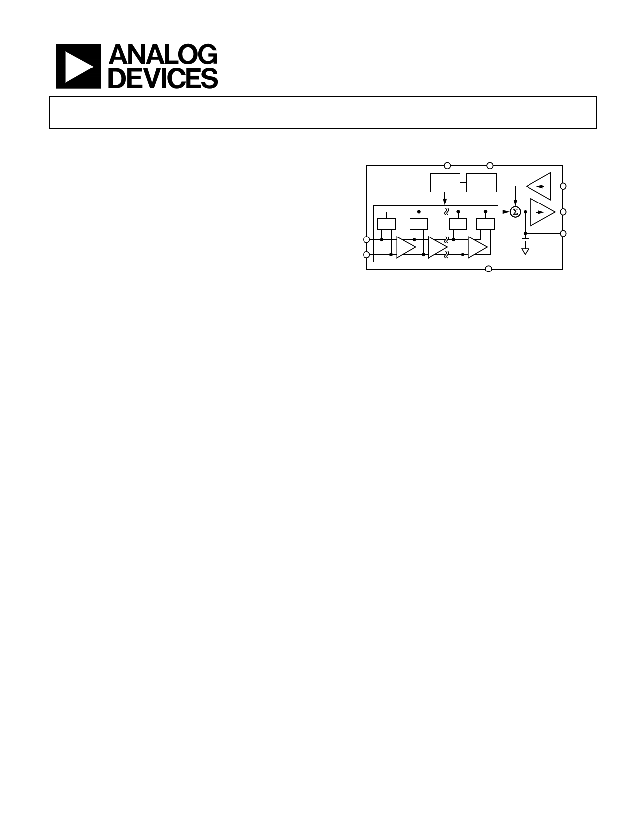
FUNCTIONAL BLOCK DIAGRAM
VPOS
TADJ
GAIN
BIAS
SLOPE
IV
VSET
INHI
INLO
DET
DET
DET DET
COMM
Figure 1.
IV
VOUT
CLPF
The feedback loop through an RF amplifier is closed via VOUT,
the output of which regulates the output of the amplifier to a
magnitude corresponding to VSET. The AD8319 provides 0 V to
(VPOS − 0.1 V) output capability at the VOUT pin, suitable for
controller applications. As a measurement device, VOUT is
externally connected to VSET to produce an output voltage,
VOUT, that is a decreasing linear-in-dB function of the RF input
signal amplitude.
The logarithmic slope is −22 mV/dB, determined by the VSET
interface. The intercept is 15 dBm (re: 50 Ω, CW input) using
the INHI input. These parameters are very stable against supply
and temperature variations.
The AD8319 is fabricated on a SiGe bipolar IC process and is
available in a 2 mm × 3 mm, 8-lead LFCSP for an operating
temperature range of −40°C to +85°C.
Rev. C
Document Feedback
Information furnished by Analog Devices is believed to be accurate and reliable. However, no
responsibilityisassumedbyAnalogDevices for itsuse,nor foranyinfringementsofpatentsor other
rights of third parties that may result from its use. Specifications subject to change without notice. No
license is granted by implication or otherwise under any patent or patent rights of Analog Devices.
Trademarksandregisteredtrademarksarethepropertyoftheirrespectiveowners.
One Technology Way, P.O. Box 9106, Norwood, MA 02062-9106, U.S.A.
Tel: 781.329.4700 ©2005–2013 Analog Devices, Inc. All rights reserved.
Technical Support
www.analog.com
1 page 
AD8319
Data Sheet
Parameter
Conditions
Min Typ
Max
f = 5.8 GHz
Input Impedance
RTADJ = 500 Ω
110||0.05
±1 dB Dynamic Range
TA = 25°C
40
Maximum Input Level
−40°C < TA < +85°C
±1 dB error
40
−3
Minimum Input Level
±1 dB error
−43
Slope1
−22
Intercept1
15
Output Voltage: High Power In
Output Voltage: Low Power In
f = 8.0 GHz
Input Impedance
PIN = −10 dBm
PIN = −40 dBm
RTADJ = open
0.57
1.25
28||0.79
±1 dB Dynamic Range
Maximum Input Level
TA = 25°C
−40°C < TA < +85°C
±1 dB error
40
31
−1
Minimum Input Level
±1 dB error
−41
Slope2
−22
Intercept2
Output Voltage: High Power In
Output Voltage: Low Power In
OUTPUT INTERFACE
PIN = −10 dBm
PIN = −40 dBm
VOUT (Pin 5)
20
0.67
1.34
Voltage Swing
VSET = 0 V; RFIN = open
VPOS − 0.1
VSET = 1.5 V; RFIN = open
10
Output Current Drive
VSET = 0 V; RFIN = open
10
Small Signal Bandwidth
RFIN = −10 dBm; from CLPF to VOUT
140
Output Noise
Fall Time
Rise Time
Video Bandwidth (or Envelope Bandwidth)
RFIN = 2.2 GHz, −10 dBm, fNOISE = 100 kHz,
CLPF = open
Input level = no signal to −10 dBm, 90% to 10%;
CLPF = 8 pF
Input level = no signal to −10 dBm, 90% to 10%;
CLPF = open; ROUT = 150 Ω
Input level = −10 dBm to no signal, 10% to 90%;
CLPF = 8 pF
Input level = −10 dBm to no signal, 10% to 90%;
CLPF = open; ROUT = 150 Ω
90
18
6
20
10
50
VSET INTERFACE
VSET (Pin 4)
Nominal Input Range
RFIN = 0 dBm; measurement mode
0.35
RFIN = −40 dBm; measurement mode
1.23
Logarithmic Scale Factor
−45
Input Resistance
RFIN = −20 dBm; controller mode; VSET = 1 V
40
TADJ INTERFACE
TADJ (Pin 6)
Input Resistance
TADJ = 0.9 V, sourcing 50 µA
40
Disable Threshold Voltage
TADJ = open
VPOS − 0.4
POWER INTERFACE
VPOS (Pin 7)
Supply Voltage
3.0 5.5
Quiescent Current
18 22
30
vs. Temperature
Disable Current
−40°C ≤ TA ≤ +85°C
TADJ = VPOS
60
200
1 Slope and intercept are determined by calculating the best fit line between the power levels of −40 dBm and −10 dBm at the specified input frequency.
2 Slope and intercept are determined by calculating the best fit line between the power levels of −34 dBm and −16 dBm at 8.0 GHz.
Unit
Ω||pF
dB
dB
dBm
dBm
mV/dB
dBm
V
V
Ω||pF
dB
dB
dBm
dBm
mV/dB
dBm
V
V
V
mV
mA
MHz
nV/√Hz
ns
ns
ns
ns
MHz
V
V
dB/V
kΩ
kΩ
V
V
mA
µA/°C
µA
Rev. C | Page 4 of 20
5 Page 
AD8319
THEORY OF OPERATION
The AD8319 is a five-stage demodulating logarithmic amplifier,
specifically designed for use in RF measurement and power control
applications at frequencies up to 10 GHz. A block diagram is
shown in Figure 21. Sharing much of its design with the AD8318
logarithmic detector/controller, the AD8319 maintains tight
intercept variability vs. temperature over a 40 dB range. Additional
enhancements over the AD8318, such as reduced RF burst
response time of 6 ns to 10 ns, 22 mA supply current, and
board space requirements of only 2 mm × 3 mm add to the low
cost and high performance benefits found in the AD8319.
VPSO
TADJ
GAIN
BIAS
SLOPE
VI
VSET
INHI
INLO
DET
DET
DET DET
IV
VOUT
CLPF
COMM
Figure 21. Block Diagram
A fully differential design, using a proprietary, high speed
SiGe process, extends high frequency performance. Input INHI
receives the signal with a low frequency impedance of nominally
500 Ω in parallel with 0.7 pF. The maximum input with ±1 dB
log conformance error is typically 0 dBm (re: 50 Ω). The noise
spectral density referred to the input is 1.15 nV/√Hz, which is
equivalent to a voltage of 118 µV rms in a 10.5 GHz bandwidth
or a noise power of −66 dBm (re: 50 Ω). This noise spectral
density sets the lower limit of the dynamic range. However, the
low end accuracy of the AD8319 is enhanced by specially shaping
the demodulating transfer characteristic to partially compensate
for errors due to internal noise. The common pin, COMM,
provides a quality low impedance connection to the PCB
ground. The package paddle, which is internally connected
to the COMM pin, should also be grounded to the PCB to
reduce thermal impedance from the die to the PCB.
Data Sheet
The logarithmic function is approximated in a piecewise fashion
by five cascaded gain stages. (For a detailed explanation of the
logarithm approximation, refer to the AD8307 data sheet.) The
cells have a nominal voltage gain of 9 dB each and a 3 dB
bandwidth of 10.5 GHz. Using precision biasing, the gain is
stabilized over temperature and supply variations. The overall
dc gain is high due to the cascaded nature of the gain stages.
An offset compensation loop is included to correct for offsets
within the cascaded cells. At the output of each of the gain
stages, a square-law detector cell is used to rectify the signal.
The RF signal voltages are converted to a fluctuating differential
current having an average value that increases with signal level.
Along with the five gain stages and detector cells, an additional
detector is included at the input of the AD8319, providing a
40 dB dynamic range in total. After the detector currents are
summed and filtered, the following function is formed at the
summing node:
ID × log10(VIN/VINTERCEPT)
(1)
where:
ID is the internally set detector current.
VIN is the input signal voltage.
VINTERCEPT is the intercept voltage (that is, when VIN = V ,INTERCEPT
the output voltage would be 0 V, if it were capable of going to 0 V).
Rev. C | Page 10 of 20
11 Page | ||
| Páginas | Total 21 Páginas | |
| PDF Descargar | [ Datasheet AD8319.PDF ] | |
Hoja de datos destacado
| Número de pieza | Descripción | Fabricantes |
| AD831 | Low Distortion Mixer | Analog Devices |
| AD8310 | 95 dB Logarithmic Amplifier | Analog Devices |
| AD8311 | 50 dB GSM PA Controller | Analog Devices |
| AD8312 | RF Detector | Analog Devices |
| Número de pieza | Descripción | Fabricantes |
| SLA6805M | High Voltage 3 phase Motor Driver IC. |
Sanken |
| SDC1742 | 12- and 14-Bit Hybrid Synchro / Resolver-to-Digital Converters. |
Analog Devices |
|
DataSheet.es es una pagina web que funciona como un repositorio de manuales o hoja de datos de muchos de los productos más populares, |
| DataSheet.es | 2020 | Privacy Policy | Contacto | Buscar |