|
|
|
PDF AD5664R Data sheet ( Hoja de datos )
| Número de pieza | AD5664R | |
| Descripción | (AD5624R - AD5664R) nanoDACs | |
| Fabricantes | Analog Devices | |
| Logotipo | ||
Hay una vista previa y un enlace de descarga de AD5664R (archivo pdf) en la parte inferior de esta página. Total 28 Páginas | ||
|
No Preview Available !
www.DataSheet4U.com
Quad, 12-/14-/16-Bit nanoDACs® with
5 ppm/°C On-Chip Reference
AD5624R/AD5644R/AD5664R
FEATURES
Low power, smallest pin-compatible, quad nanoDACs
AD5664R: 16 bits
AD5644R: 14 bits
AD5624R: 12 bits
User selectable external or internal reference
External reference default
On-chip 1.25 V/2.5 V, 5 ppm/°C reference
10-lead MSOP and 3 mm × 3 mm LFCSP_WD
2.7 V to 5.5 V power supply
Guaranteed monotonic by design
Power-on reset to zero scale
Per channel power-down
Serial interface, up to 50 MHz
APPLICATIONS
Process control
Data acquisition systems
Portable battery-powered instruments
Digital gain and offset adjustment
Programmable voltage and current sources
Programmable attenuators
GENERAL DESCRIPTION
The AD5624R/AD5644R/AD5664R, members of the nanoDAC
family, are low power, quad, 12-/14-/16-bit buffered voltage-out
DACs. All devices operate from a single 2.7 V to 5.5 V supply
and are guaranteed monotonic by design.
The AD5624R/AD5644R/AD5664R have an on-chip reference.
The AD56x4R-3 has a 1.25 V, 5 ppm/°C reference, giving a full-
scale output range of 2.5 V; the AD56x4R-5 has a 2.5 V,
5 ppm/°C reference giving a full-scale output range of 5 V. The
on-chip reference is off at power-up allowing the use of an
external reference and all devices can be operated from a single
2.7 V to 5.5 V supply. The internal reference is enabled via a
software write.
The part incorporates a power-on reset circuit that ensures the
DAC output powers up to 0 V and remains there until a valid
write takes place. The part contains a per-channel power-down
feature that reduces the current consumption of the device to
480 nA at 5 V and provides software-selectable output loads
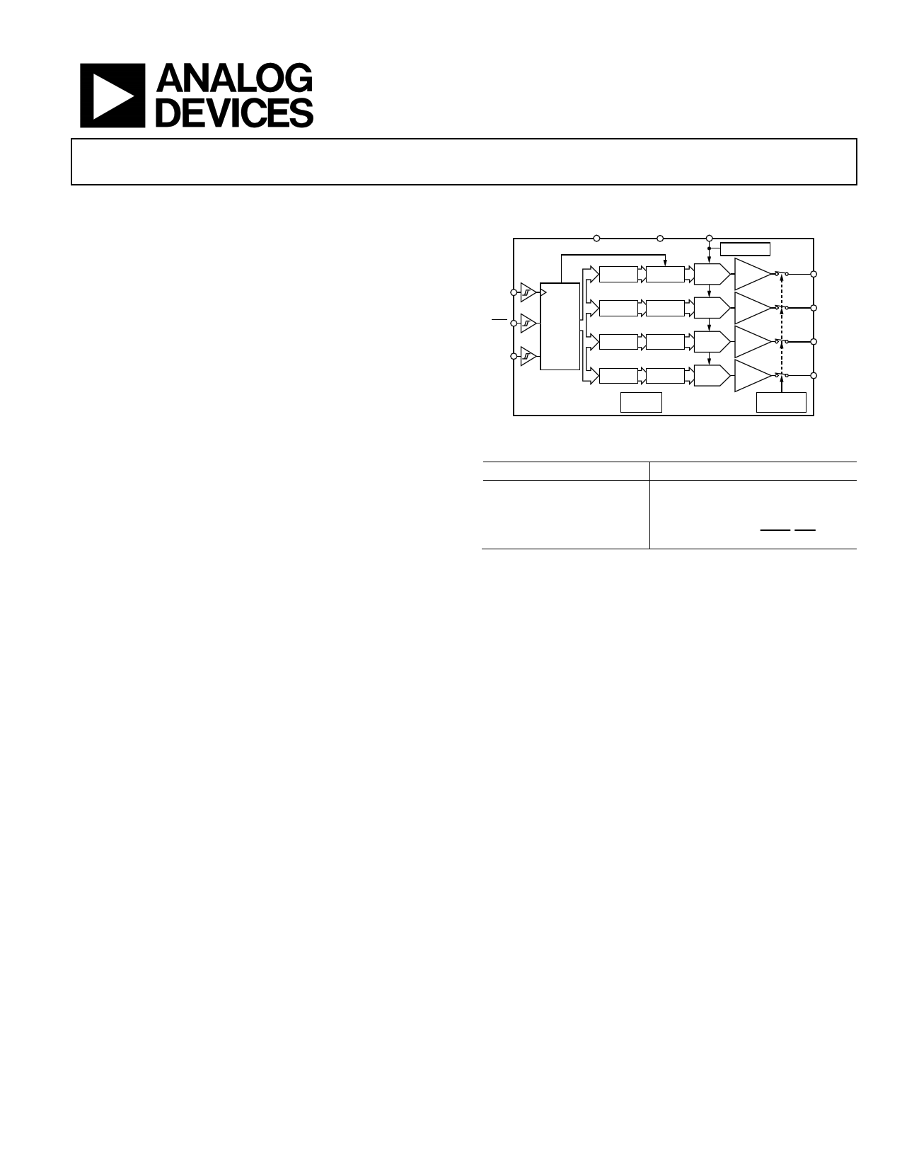
FUNCTIONAL BLOCK DIAGRAM
VDD
GND
VREFIN/VREFOUT
AD5624R/AD5644R/AD5664R
1.25V/2.5V REF
SCLK
SYNC
DIN
INTERFACE
LOGIC
INPUT
REGISTER
DAC
REGISTER
STRING
DAC A
BUFFER
INPUT
REGISTER
DAC
REGISTER
STRING
DAC B
BUFFER
INPUT
REGISTER
DAC
REGISTER
STRING
DAC C
BUFFER
INPUT
REGISTER
DAC
REGISTER
STRING
DAC D
BUFFER
VOUTA
VOUTB
VOUTC
VOUTD
POWER-ON
RESET
POWER-DOWN
LOGIC
Figure 1.
Table 1. Related Devices
Part No.
AD5624/AD5664
AD5666
Description
2.7 V to 5.5 V quad, 12-/16-bit
DACs, external reference
2.7 V to 5.5 V quad 16-bit DAC,
internal reference, LDAC, CLR pins
while in power-down mode. The low power consumption of
this part in normal operation makes it ideally suited to portable
battery-operated equipment.
The AD5624R/AD5644R/AD5664R use a versatile 3-wire serial
interface that operates at clock rates up to 50 MHz, and is
compatible with standard SPI®, QSPI™, MICROWIRE™, and
DSP interface standards. The on-chip precision output amplifier
enables rail-to-rail output swing.
PRODUCT HIGHLIGHTS
1. Quad 12-/14-/16-bit DACs.
2. On-chip 1.25 V/2.5 V, 5 ppm/°C reference.
3. Available in 10-lead MSOP and 10-lead, 3 mm × 3 mm,
LFCSP_WD.
4. Low power, typically consumes 1.32 mW at 3 V and
2.25 mW at 5 V.
Rev. A
Information furnished by Analog Devices is believed to be accurate and reliable. However, no
responsibility is assumed by Analog Devices for its use, nor for any infringements of patents or other
rights of third parties that may result from its use. Specifications subject to change without notice. No
license is granted by implication or otherwise under any patent or patent rights of Analog Devices.
Trademarksandregisteredtrademarksarethepropertyoftheirrespectiveowners.
One Technology Way, P.O. Box 9106, Norwood, MA 02062-9106, U.S.A.
Tel: 781.329.4700
www.analog.com
Fax: 781.461.3113
©2006 Analog Devices, Inc. All rights reserved.
1 page 
AD5624R/AD5644R/AD5664R
AD5624R-3/AD5644R-3/AD5664R-3
VDD = 2.7 V to 3.6 V; RL = 2 kΩ to GND; CL = 200 pF to GND; VREFIN = VDD; all specifications TMIN to TMAX, unless otherwise noted.
Table 3.
Parameter
STATIC PERFORMANCE2
AD5664R
Resolution
Relative Accuracy
Differential Nonlinearity
AD5644R
Resolution
Relative Accuracy
Differential Nonlinearity
AD5624R
Resolution
Relative Accuracy
Differential Nonlinearity
Zero-Code Error
Offset Error
Full-Scale Error
Gain Error
Zero-Code Error Drift
Gain Temperature Coefficient
DC Power Supply Rejection
Ratio
DC Crosstalk
(External Reference)
Min
16
14
12
DC Crosstalk
(Internal Reference)
OUTPUT CHARACTERISTICS3
Output Voltage Range
Capacitive Load Stability
DC Output Impedance
Short-Circuit Current
Power-Up Time
REFERENCE INPUTS
Reference Current
Reference Input Range
Reference Input Impedance
REFERENCE OUTPUT
Output Voltage
Reference TC3
Output Impedance
0
0
1.247
B Grade1
Typ Max
±8 ±16
±1
±2 ±4
±0.5
±0.5
2
±1
−0.1
±2
±2.5
−100
10
10
5
25
20
10
2
10
0.5
30
4
170
26
±5
±10
7.5
±1
±0.25
10
±10
±1
±1.5
VDD
200
VDD
1.253
±15
Unit
Bits
LSB
LSB
Bits
LSB
LSB
Bits
LSB
LSB
mV
mV
% of FSR
% of FSR
μV/°C
ppm
dB
μV
μV/mA
μV
μV
μV/mA
μV
V
nF
nF
Ω
mA
μs
μA
V
kΩ
V
ppm/°C
ppm/°C
kΩ
Conditions/Comments
Guaranteed monotonic by design
Guaranteed monotonic by design
Guaranteed monotonic by design
All zeroes loaded to DAC register
All ones loaded to DAC register
Of FSR/°C
DAC code = midscale; VDD = 3 V ± 10%
Due to full-scale output change,
RL = 2 kΩ to GND or VDD
Due to load current change
Due to powering down (per channel)
Due to full-scale output change,
RL = 2 kΩ to GND or VDD
Due to load current change
Due to powering down (per channel)
RL = ∞
RL = 2 kΩ
VDD = 3 V
Coming out of power-down mode; VDD = 3 V
VREF = VDD = 3.6 V
At ambient
MSOP package models
LFCSP package models
Rev. A | Page 5 of 28
5 Page 
10
VDD = 5V
8 VREFOUT = 2.5V
TA = 25°C
6
4
2
0
–2
–4
–6
–8
–10
CODE
Figure 10. INL AD5664R-5, Internal Reference
AD5624R/AD5644R/AD5664R
1.0
VDD = 5V
0.8 VREFOUT = 2.5V
TA = 25°C
0.6
0.4
0.2
0
–0.2
–0.4
–0.6
–0.8
–1.0
CODE
Figure 13. DNL AD5664R-5, Internal Reference
4
VDD = 5V
3
VREFOUT = 2.5V
TA = 25°C
2
1
0
–1
–2
–3
–4
CODE
Figure 11. INL AD5644R-5, Internal Reference
0.5
VDD = 5V
0.4 VREFOUT = 2.5V
TA = 25°C
0.3
0.2
0.1
0
–0.1
–0.2
–0.3
–0.4
–0.5
CODE
Figure 14. DNL AD5644R-5, Internal Reference
1.0
VDD = 5V
0.8 VREFOUT = 2.5V
TA = 25°C
0.6
0.4
0.2
0
–0.2
–0.4
–0.6
–0.8
–1.0
0
500 1000 1500 2000 2500 3000 3500 4000
CODE
Figure 12. INL AD5624R-5, Internal Reference
0.20
0.15
0.10
VDD = 5V
VREFOUT = 2.5V
TA = 25°C
0.05
0
–0.05
–0.10
–0.15
–0.20
0
500 1000 1500 2000 2500 3000 3500
CODE
Figure 15. DNL AD5624R-5, Internal Reference
4000
Rev. A | Page 11 of 28
11 Page | ||
| Páginas | Total 28 Páginas | |
| PDF Descargar | [ Datasheet AD5664R.PDF ] | |
Hoja de datos destacado
| Número de pieza | Descripción | Fabricantes |
| AD5664 | (AD5624 / AD5664) nanoDACs | Analog Devices |
| AD5664R | (AD5624R - AD5664R) nanoDACs | Analog Devices |
| Número de pieza | Descripción | Fabricantes |
| SLA6805M | High Voltage 3 phase Motor Driver IC. |
Sanken |
| SDC1742 | 12- and 14-Bit Hybrid Synchro / Resolver-to-Digital Converters. |
Analog Devices |
|
DataSheet.es es una pagina web que funciona como un repositorio de manuales o hoja de datos de muchos de los productos más populares, |
| DataSheet.es | 2020 | Privacy Policy | Contacto | Buscar |