|
|
|
PDF CD4049BMS Data sheet ( Hoja de datos )
| Número de pieza | CD4049BMS | |
| Descripción | CMOS Hex Buffer/Converter | |
| Fabricantes | Intersil Corporation | |
| Logotipo | ||
Hay una vista previa y un enlace de descarga de CD4049BMS (archivo pdf) en la parte inferior de esta página. Total 7 Páginas | ||
|
No Preview Available !
www.DataSheet4U.com
Data Sheet
CD4049UBMS
December 1992
File Number 3315
CMOS Hex Buffer/Converter
Features
The CD4049UBMS is an inverting hex buffer and features
logic level conversion using only one supply (voltage (VCC).
The input signal high level (VIH) can exceed the VCC supply
voltage when this device is used for logic level conversions.
This device is intended for use as CMOS to DTL/TTL
converters and can drive directly two DTL/TTL loads. (VCC
= 5V, VOL ≤ 0.4V, and IOL ≥ 3.3mA.
• High Voltage Type (20V Rating)
• Inverting Type
• High Sink Current for Driving 2 TTL Loads
• High-to-Low Level Logic Conversion
• 100% Tested for Quiescent Current at 20V
The CD4049UBMS is designated as replacement for
CD4009UB. Because the CD4049UBMS requires only one
• Maximum Input Current of 1µA at 18V Over Full Pack-
age Temperature Range; 100nA at 18V and +25oC
power supply, it is preferred over the CD4009UB and
CD4010B and should be used in place of the CD4009UB in
• 5V, 10V and 15V Parametric Ratings
all inverter, current driver, or logic level conversion applica-
tions. In these applications the CD4049UBMS is pin compat-
Applications
ible with the CD4009UB, and can be substituted for this
device in existing as well as in new designs. Terminal No. 16
• CMOS to DTL/TTL Hex Converter
is not connected internally on the CD4049UBMS, therefore,
• CMOS Current “Sink” or “Source” Driver
connection to this terminal is of no consequence to circuit
operation. For applications not requiring high sink current or
• CMOS High-to-Low Logic Level Converter
voltage conversion, the CD4069UB Hex Inverter is recom-
mended.
Pinout
CD4049UBMS
The CD4049UBMS is supplied in these 16 lead outline pack-
TOP VIEW
ages:
www.DataSheet4U.comBraze Seal DIP
H4S
VCC 1
G=A 2
16 NC
15 L = F
Frit Seal DIP
H1E
A3
14 F
Ceramic Flatpack H3X
H=B 4
B5
13 NC
12 K = E
I=C 6
11 E
C7
10 J = D
VSS 8
9D
Functional Diagram
3
A
5
B
7
C
VCC
VSS
1
8
NC = 13
NC = 16
9
D
11
E
14
F
2
G=A
4
H=B
6
I=C
10
J=D
12
K=E
15
L=F
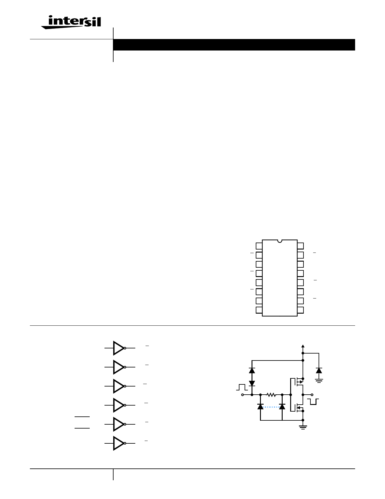
Schematic
VCC
R
IN
P
OUT
N
VSS
FIGURE 1. SCHEMATIC DIAGRAM, 1 OF 6 IDENTICAL UNITS
1 CAUTION: These devices are sensitive to electrostatic discharge; follow proper IC Handling Procedures.
1-888-INTERSIL or 321-724-7143 | Copyright © Intersil Corporation 1999
www.DataSheet4U.com
1 page 
www.DataSheet4U.com
CD4049UBMS
TABLE 6. APPLICABLE SUBGROUPS
CONFORMANCE GROUP
MIL-STD-883
METHOD
GROUP A SUBGROUPS
Interim Test 2 (Post Burn-In)
100% 5004
1, 7, 9
PDA (Note 1)
100% 5004
1, 7, 9, Deltas
Interim Test 3 (Post Burn-In)
100% 5004
1, 7, 9
PDA (Note 1)
100% 5004
1, 7, 9, Deltas
Final Test
100% 5004
2, 3, 8A, 8B, 10, 11
Group A
Sample 5005
1, 2, 3, 7, 8A, 8B, 9, 10, 11
Group B
Subgroup B-5
Sample 5005
1, 2, 3, 7, 8A, 8B, 9, 10, 11, Deltas
Subgroup B-6
Sample 5005
1, 7, 9
Group D
Sample 5005
1, 2, 3, 8A, 8B, 9
NOTE: 1. 5% Parameteric, 3% Functional; Cumulative for Static 1 and 2.
CONFORMANCE GROUPS
Group E Subgroup 2
TABLE 7. TOTAL DOSE IRRADIATION
MIL-STD-883
METHOD
TEST
PRE-IRRAD
POST-IRRAD
5005
1, 7, 9
Table 4
READ AND RECORD
IDD, IOL5, IOH5A
IDD, IOL5, IOH5A
Subgroups 1, 2, 3, 9, 10, 11
Subgroups 1, 2 3
READ AND RECORD
PRE-IRRAD
POST-IRRAD
1, 9 Table 4
TABLE 8. BURN-IN AND IRRADIATION TEST CONNECTIONS
OSCILLATOR
FUNCTION
OPEN
GROUND
VDD
9V ± -0.5V
50kHz
25kHz
Static Burn-In 1 (Note 1) 2, 4, 6, 10, 12, 13, 15 3, 5, 7-9, 11-14
1, 16
Static Burn-In 2 (Note 1) 2, 4, 6, 10, 12, 13, 15
www.DataSheet4U.comDynamic Burn-In (Note 3)
13
8 1, 3, 5, 7, 9, 11, 14, 16
8
1, 16
2, 4, 6, 10, 12, 15 3, 5, 7, 9, 11, 14
Irradiation (Note 2)
2, 4, 6, 10, 12, 13, 15, 16
8
1, 3, 5, 7, 9, 11, 14
NOTE:
1. Each pin except pin 1, pin 16, and GND will have a series resistor of 10K ± 5%, VDD = 18V ± 0.5V
2. Each pin except pin 1, pin 16, and GND will have a series resistor of 47K ± 5%; Group E, Subgroup 2, sample size is 4 dice/wafer, 0 failures, VDD
= 10V ± 0.5V
3. Each pin except pin 1, pin 16, and GND will have a series resistor of 4.75K ± 5%, VDD = 18V ± 0.5V
Typical Performance Characteristics
AMBIENT TEMPERATURE (TA) = +25oC
SUPPLY VOLTAGE (VCC) = 5V
5
4
MINIMUM
MAXIMUM
3
2
1
0 12 34
INPUT VOLTAGE (VI) (V)
FIGURE 2. MINIMUM AND MAXIMUM VOLTAGE TRANSFER
CHARACTERISTICS
AMBIENT TEMPERATURE (TA) = +25oC
70
15V 10V
60
50
40
30
GATE-TO-SOURCE VOLTAGE (VGS) = 5V
20
10
0 12 34 5 67 8
DRAIN-TO-SOURCE VOLTAGE (VDS) (V)
FIGURE 3. TYPICAL OUTPUT LOW (SINK) CURRENT
CHARACTERISTICS
5
www.DataSheet4U.com
5 Page | ||
| Páginas | Total 7 Páginas | |
| PDF Descargar | [ Datasheet CD4049BMS.PDF ] | |
Hoja de datos destacado
| Número de pieza | Descripción | Fabricantes |
| CD4049BMS | CMOS Hex Buffer/Converter | Intersil Corporation |
| Número de pieza | Descripción | Fabricantes |
| SLA6805M | High Voltage 3 phase Motor Driver IC. |
Sanken |
| SDC1742 | 12- and 14-Bit Hybrid Synchro / Resolver-to-Digital Converters. |
Analog Devices |
|
DataSheet.es es una pagina web que funciona como un repositorio de manuales o hoja de datos de muchos de los productos más populares, |
| DataSheet.es | 2020 | Privacy Policy | Contacto | Buscar |