|
|
|
PDF 2SK3569 Data sheet ( Hoja de datos )
| Número de pieza | 2SK3569 | |
| Descripción | TOSHIBA Field Effect Transistor Silicon N Channel MOS Type (PIE-MOSVI) | |
| Fabricantes | Toshiba Semiconductor | |
| Logotipo | ||
Hay una vista previa y un enlace de descarga de 2SK3569 (archivo pdf) en la parte inferior de esta página. Total 6 Páginas | ||
|
No Preview Available !
www.DataSheet4U.com
2SK3569
TOSHIBA Field Effect Transistor Silicon N Channel MOS Type (π-MOSVI)
2SK3569
Switching Regulator Applications
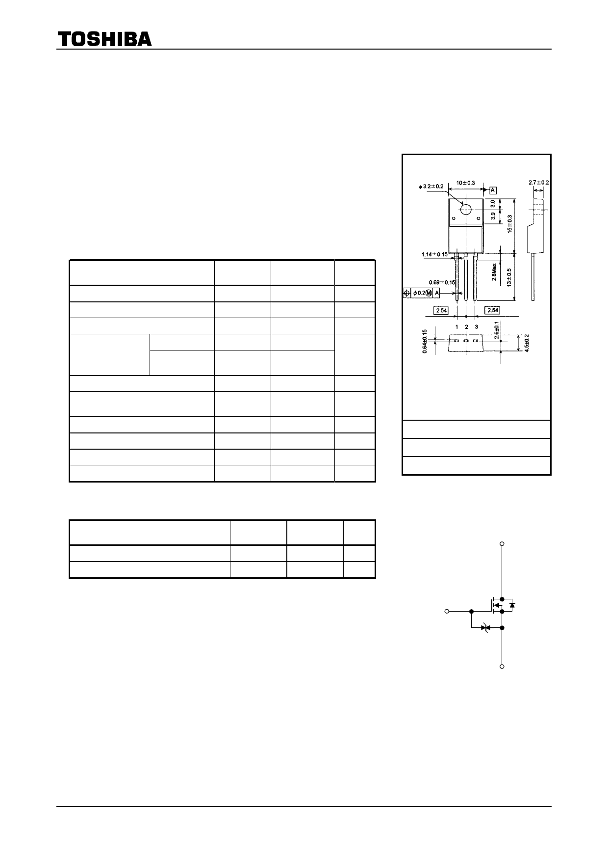
Unit: mm
• Low drain-source ON resistance: RDS (ON) = 0.54 (typ.)
• High forward transfer admittance: |Yfs| = 8.5S (typ.)
• Low leakage current: IDSS = 100 A (VDS = 600 V)
• Enhancement-mode: Vth = 2.0~4.0 V (VDS = 10 V, ID = 1 mA)
Maximum Ratings (Ta = 25°C)
Characteristics
Drain-source voltage
Drain-gate voltage (RGS = 20 kΩ)
Gate-source voltage
Drain current
DC (Note 1)
Pulse (t = 1 ms)
(Note 1)
Drain power dissipation (Tc = 25°C)
Single pulse avalanche energy
(Note 2)
Avalanche current
Repetitive avalanche energy (Note 3)
Channel temperature
Storage temperature range
Symbol
VDSS
VDGR
VGSS
ID
IDP
PD
EAS
IAR
EAR
Tch
Tstg
Thermal Characteristics
Rating
600
600
±30
10
40
45
363
10
4.5
150
-55~150
Unit
V
V
V
A
W
mJ
A
mJ
°C
°C
1: Gate
2: Drain
3: Source
JEDEC
―
JEITA
SC-67
TOSHIBA
2-10U1B
Weight : 1.7 g (typ.)
Characteristics
Symbol
Max Unit
Thermal resistance, channel to case
Thermal resistance, channel to ambient
Rth (ch-c)
Rth (ch-a)
2.78
62.5
°C/W
°C/W
Note 1: Please use devices on conditions that the channel temperature is below 150°C.
Note 2: VDD = 90 V, Tch = 25°C(initial), L = 6.36 mH, IAR = 10 A, RG = 25 Ω
Note 3: Repetitive rating: Pulse width limited by maximum channel temperature
1
This transistor is an electrostatic sensitive device. Please handle with caution.
2
3
www.DataSheet4U.com
1
2004-03-04
1 page 
www.DataSheet4U.com
2SK3569
rth – tw
10
1 Duty=0.5
0.2
0.1 0.1
0.05
0.02
0.01
0.01
0.001
10
100
SINGLE PULSE
1 10 100
PULSE WIDTH tw (s)
PDM
t
T
Duty = t/T
Rth (ch-c) = 2.78°C/W
1 10
SAFE OPERATING AREA
100
ID max (PULSED) *
ID max (CONTINUOUS) *
10
100 µs *
1 ms *
DC OPERATION
Tc = 25°C
1
0.1
SINGLE NONREPETITIVE PULSE
Tc=25
CURVES MUST BE DERATED
LINEARLY WITH INCREASE IN
0.01 TEMPERATURE.
1 10
VDSS max
100
1000
DRAIN-SOURCE VOLTAGE VDS (V)
EAS – Tch
500
400
300
200
100
0
25 50
75 100 125 150
CHANNEL TEMPERATURE (INITIAL)
Tch (°C)
15 V
−15 V
BVDSS
IAR
VDD
VDS
TEST CIRCUIT
WAVE FORM
RG = 25 Ω
VDD = 90 V, L = 6.36mH
ΕAS
=
1
2
⋅L ⋅I2
⋅
BVDSS
BVDSS − VDD
www.DataSheet4U.com
5
2004-03-04
5 Page | ||
| Páginas | Total 6 Páginas | |
| PDF Descargar | [ Datasheet 2SK3569.PDF ] | |
Hoja de datos destacado
| Número de pieza | Descripción | Fabricantes |
| 2SK3560 | Silicon N-channel power MOSFET For PDP/For high-speed switching | Panasonic Semiconductor |
| 2SK3560 | Silicon N-channel power MOSFET | Kexin |
| 2SK3561 | Silicon N Channel MOS Type Field Effect Transistor | Toshiba |
| 2SK3561 | Silicon N Channel MOS Type Field Effect Transistor | Toshiba Semiconductor |
| Número de pieza | Descripción | Fabricantes |
| SLA6805M | High Voltage 3 phase Motor Driver IC. |
Sanken |
| SDC1742 | 12- and 14-Bit Hybrid Synchro / Resolver-to-Digital Converters. |
Analog Devices |
|
DataSheet.es es una pagina web que funciona como un repositorio de manuales o hoja de datos de muchos de los productos más populares, |
| DataSheet.es | 2020 | Privacy Policy | Contacto | Buscar |