|
|
|
PDF A6801 Data sheet ( Hoja de datos )
| Número de pieza | A6801 | |
| Descripción | DABiC-5 Latched Sink Drivers | |
| Fabricantes | Allegro MicroSystems | |
| Logotipo | ||
Hay una vista previa y un enlace de descarga de A6801 (archivo pdf) en la parte inferior de esta página. Total 11 Páginas | ||
|
No Preview Available !
A6800 and A6801
DABiC-5 Latched Sink Drivers
Features and Benefits
▪ 3.3 to 5 V logic supply range
▪ Up to 10 MHz data input rate
▪ High-voltage, high-current outputs
▪ Darlington current-sink outputs, with improved low-saturation
voltages
▪ CMOS, TTL compatible inputs
▪ Output transient protection
▪ Internal pull-down resistors
▪ Low-power CMOS latches
Packages
A6800
14-pin 7.62 mm DIP
(A package)
A6800
14-pin SOICN
(L package)
A6801
28-pin PLCC
(EP package)
Approximate scale 1:1
A6801
24-pin SOICW
(LW package)
Description
The A6800 and A6801 latched-input BiMOS ICs merge
high-current, high-voltage outputs with CMOS logic. The
CMOS input section consists of 4 or 8 data (D type) latches
with associated common CLEAR, STROBE, and OUTPUT
ENABLE circuitry. The power outputs are bipolar NPN
Darlingtons. This merged technology provides versatile,
flexible interface. These BiMOS power interface ICs greatly
benefit the simplification of computer or microproces-
sor I/O. The A6800 ICs each contain four latched drivers.
A6801 ICs contain eight latched drivers.
The CMOS inputs are compatible with standard CMOS
circuits. TTL circuits may mandate the addition of input
pull-up resistors. The bipolar Darlington outputs are suitable
for directly driving many peripheral/power loads: relays,
lamps, solenoids, small DC motors, and so forth.
All devices have open-collector outputs and integral diodes
for inductive load transient suppression. The output transis-
tors are capable of sinking 600 mA and can withstand at
least 50 V in the off state. Because of limitations on package
power dissipation, the simultaneous operation of all driv-
ers at maximum rated current can only be accomplished
by a reduction in duty cycle. Outputs may be paralleled for
higher load current capability.
Continued on the next page…
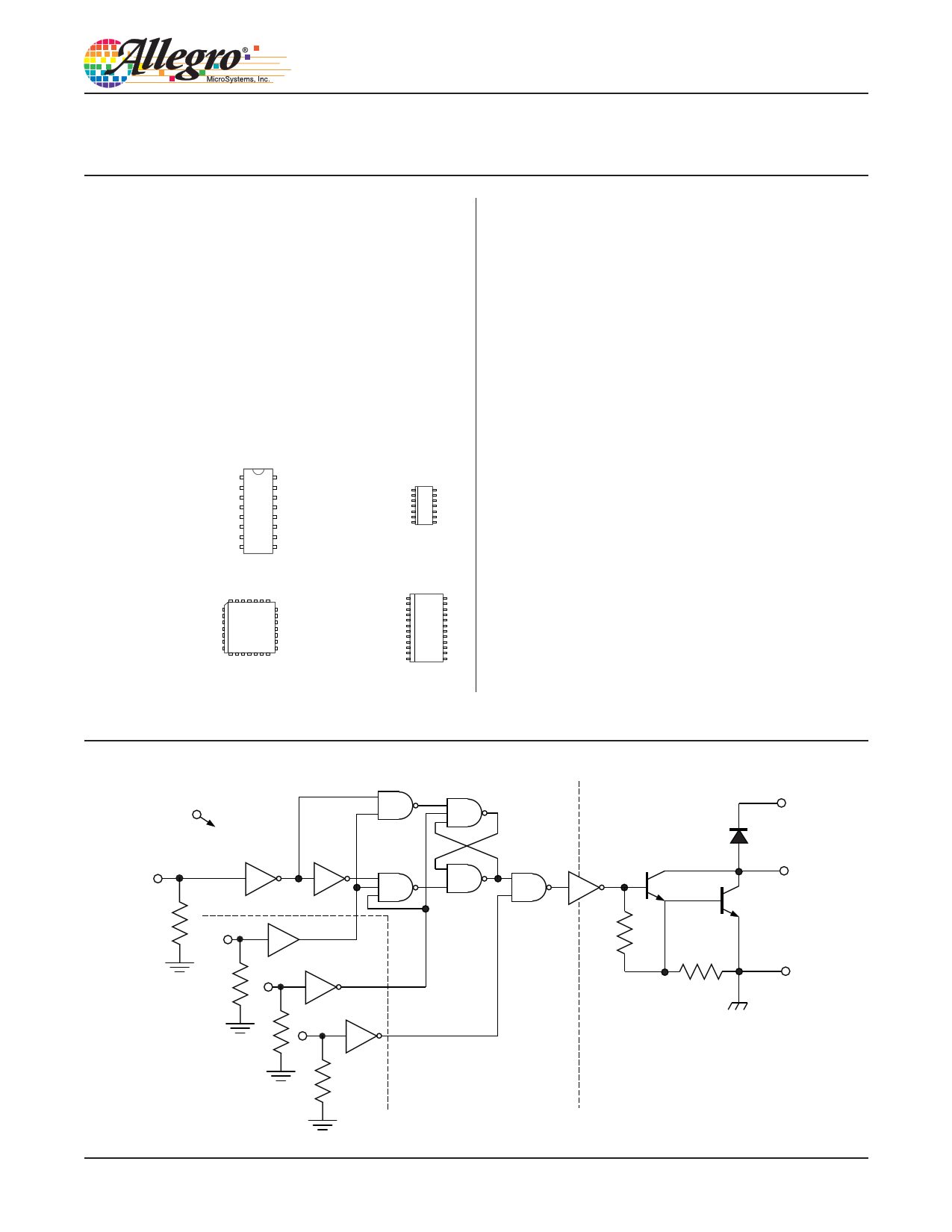
S UP P LY
V DD
IN N
Functional Block Diagram
C OMMON
OUT N
S TR OBE
CLE AR
OUTPUT E NABLE
C OMMON MOS C ONTR OL
TYP IC AL MOS LATC H
GR OUND
TYPIC AL BIPOLAR DR IVE
26180.110H
1 page 
A6800 and
A6801
DABiC-5 Latched Sink Drivers
Timing Requirements and Specifications
(Logic Levels are VDD and Ground)
CLEAR
STROBE
INN
OUTN
A CB
H
CB
DE
G
F
A CB
H
E
OUTPUT ENABLE
OUT N
50%
t dis(BQ)
10%
HIGH = ALL OUTPUTS DISABLED (OFF)
t en(BQ)
tr
DATA
tf
90%
50%
Key Description
A Minimum data active time before Strobe enabled (Data Set-Up Time)
B Minimum data active time after Strobe disabled (Data Hold Time)
C Minimum Strobe pulse width
D
E
F
G
H
tdis(BQ)
ten(BQ)
Maximum time between Strobe activation and transition from output on to output off*
Maximum time between Strobe activation and transition from output off to output on*
Maximum time between Clear activation and transition from output on to output off*
Minimum Clear pulse width
Minimum data pulse width
Output Enable to output off delay*
Output Enable to output on delay*
*Conditions for output transition testing are: VCC = 50 V, VDD = 5 V, R1 = 500 Ω, C1 ≤ 30 pF.
Time (ns)
25
25
50
500
500
500
50
100
500
500
NOTE: Information present at an input is transferred
to its latch when the STROBE is high. A high CLEAR
input will set all latches to the output off condition
regardless of the data or STROBE input levels. A high
OUTPUT ENABLE will set all outputs to the off con-
tdition, regardless of any other input conditions. When
the OUTPUT ENABLE is low, the outputs depend on
the state of their respective latches.
Allegro MicroSystems, Inc.
115 Northeast Cutoff
Worcester, Massachusetts 01615-0036 U.S.A.
1.508.853.5000; www.allegromicro.com
5
5 Page 
A6800 and
A6801
DABiC-5 Latched Sink Drivers
Copyright ©2003-2009, Allegro MicroSystems, Inc.
The products described here are manufactured under one or more U.S. patents or U.S. patents pending.
Allegro MicroSystems, Inc. reserves the right to make, from time to time, such departures from the detail specifications as may be required to per-
mit improvements in the performance, reliability, or manufacturability of its products. Before placing an order, the user is cautioned to verify that the
information being relied upon is current.
Allegro’s products are not to be used in life support devices or systems, if a failure of an Allegro product can reasonably be expected to cause the
failure of that life support device or system, or to affect the safety or effectiveness of that device or system.
The information included herein is believed to be accurate and reliable. However, Allegro MicroSystems, Inc. assumes no responsibility for its use;
nor for any infringement of patents or other rights of third parties which may result from its use.
For the latest version of this document, visit our website:
www.allegromicro.com
Allegro MicroSystems, Inc.
115 Northeast Cutoff
Worcester, Massachusetts 01615-0036 U.S.A.
1.508.853.5000; www.allegromicro.com
11
11 Page | ||
| Páginas | Total 11 Páginas | |
| PDF Descargar | [ Datasheet A6801.PDF ] | |
Hoja de datos destacado
| Número de pieza | Descripción | Fabricantes |
| A6800 | (A6800 / A6801) DABiC-5 Latched Sink Drivers | Allegro MicroSystems |
| A6801 | GIGABIT DUAL TRANSFORMERS | Pulse |
| A6801 | DABiC-5 Latched Sink Drivers | Allegro MicroSystems |
| A6802 | GIGABIT DUAL TRANSFORMERS | Pulse |
| Número de pieza | Descripción | Fabricantes |
| SLA6805M | High Voltage 3 phase Motor Driver IC. |
Sanken |
| SDC1742 | 12- and 14-Bit Hybrid Synchro / Resolver-to-Digital Converters. |
Analog Devices |
|
DataSheet.es es una pagina web que funciona como un repositorio de manuales o hoja de datos de muchos de los productos más populares, |
| DataSheet.es | 2020 | Privacy Policy | Contacto | Buscar |