|
|
|
PDF DS1374 Data sheet ( Hoja de datos )
| Número de pieza | DS1374 | |
| Descripción | 32-Bit Binary Counter Watchdog RTC | |
| Fabricantes | Maxim Integrated Products | |
| Logotipo | ||
Hay una vista previa y un enlace de descarga de DS1374 (archivo pdf) en la parte inferior de esta página. Total 16 Páginas | ||
|
No Preview Available !
Rev 2; 9/05
I2C,h3ee2t-T4BUrii.tccokBmlienaCrhyaCrgoeurnatenrdWRaetscehtdIongpuRtT/OCuwtpituhtGeneral Description
taSThe DS1374 is a 32-bit binary counter designed to contin-
uously count time in seconds. An additional counter gen-
aerates a periodic alarm or serves as a watchdog timer. If
.Ddisabled, this counter can be used as 3 bytes of non-
wvolatile (NV) RAM. Separate output pins are provided for
an interrupt and a square wave at one of four selectable
wfrequencies. A precision temperature-compensated refer-
wence and comparator circuit monitor the status of VCC to
mdetect power failures, provide a reset output, and auto-
matically switch to the backup supply when necessary.
oAdditionally, the reset pin is monitored as a pushbutton
input for externally generating a reset. The device is pro-
.cgrammed serially through an I2C™ serial interface.
t4UPortable Instruments
Point-of-Sale Equipment
eMedical Equipment
eTelecommunications
Applications
ShI2C is a trademark of Philips Corp. Purchase of I2C compo-
nents of Maxim Integrated Products, Inc., or one of its subli-
tacensed Associated Companies, conveys a license under the
Philips I2C Patent Rights to use these components in an I2C
system, provided that the system conforms to the I2C Standard
aSpecification as defined by Philips.
.DPin Configurations appear at the end of the data sheet.
Features
♦ 32-Bit Binary Counter
♦ Second Binary Counter Provides Time-of-Day
Alarm, Watchdog Timer, or NV RAM
♦ Separate Square-Wave and Interrupt Output Pins
♦ I2C Serial Interface
♦ Automatic Power-Fail Detect and Switch Circuitry
♦ Single-Pin Pushbutton Reset Input/Open-Drain
Reset Output
♦ Low-Voltage Operation
♦ Trickle-Charge Capability
♦ -40°C to +85°C Operating Temperature Range
♦ 10-Pin µSOP, 16-Pin SO
♦ Available in a Surface-Mount Package with an
Integrated Crystal (DS1374C)
♦ Underwriters Laboratory (UL) Recognized
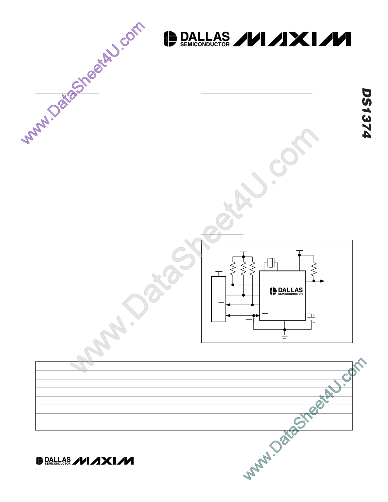
Typical Operating Circuit
RPU = tr/CB VCC
RPU RPU
VCC
CPU
INT
RST
N.O.
PUSHBUTTON
RESET
CRYSTAL
VCC
X1 X2
SCL
VCC
SQW
SDA
DS1374
INT
RST
VBACKUP
GND
PRIMARY
BATTERY,
RECHARGEABLE
BATTERY, OR
SUPER CAPACITOR
wwPART
TEMP RANGE
VOLTAGE (V)
w omDS1374C-18
-40°C to +85°C
1.8
.cDS1374C-18+
-40°C to +85°C
1.8
UDS1374C-3
-40°C to +85°C
3.0
t4DS1374C-3+
-40°C to +85°C
3.0
eDS1374C-33
-40°C to +85°C
3.3
eDS1374C-33+
-40°C to +85°C
3.3
hDS1374C-33/T&R
-40°C to +85°C
3.3
taSOrdering Information continued at end of data sheet.
+ Denotes a lead-free/RoHS-compliant device.
a* A "+" anywhere on the top mark denotes a lead-free device.
Ordering Information
PIN-PACKAGE
16 SO (300 mils)
16 SO (300 mils)
16 SO (300 mils)
16 SO (300 mils)
16 SO (300 mils)
16 SO (300 mils)
16 SO (300 mils)/Tape and Reel
TOP MARK*
DS1374C-18
DS1374C-18
DS1374C-3
DS1374C-3
DS1374C-33
DS1374C-33
DS1374C-33
w.D______________________________________________ Maxim Integrated Products 1
wFor pricing, delivery, and ordering information, please contact Maxim/Dallas Direct! at
w1-888-629-4642, or visit Maxim’s website at www.maxim-ic.com.
1 page 
I2C, 32-Bit Binary Counter Watchdog RTC with
Trickle Charger and Reset Input/Output
POWER-UP/POWER-DOWN CHARACTERISTICS
(TA = -40°C to +85°C) (Figure 3)
PARAMETER
VCC Detect to Recognize Inputs
(VCC Rising)
SYMBOL
tRPU (Note 23)
CONDITIONS
VCC Fall Time; VPF(MAX) to
VPF(MIN)
VCC Rise Time; VPF(MIN) to
VPF(MAX)
tF
tR
MIN TYP MAX UNITS
250 ms
300 µs
0 µs
WARNING: Under no circumstances are negative undershoots, of any amplitude, allowed when the device is in write protection.
Note 1: Limits at -40°C are guaranteed by design and not production tested.
Note 2: All voltages are referenced to ground.
Note 3: VBACKUP should not exceed VCC MAX or 3.7V, whichever is greater.
Note 4: The use of the 250Ω trickle-charge resistor is not allowed at VCC > 3.63V and should not be enabled.
Note 5: Measured at VCC = typ, VBACKUP = 0V, register 09h = A5h.
Note 6: Measured at VCC = typ, VBACKUP = 0V, register 09h = A6h.
Note 7: Measured at VCC = typ, VBACKUP = 0V, register 09h = A7h.
Note 8: SCL only.
Note 9: SDA and SQW and INT.
Note 10: The RST pin has an internal 50kΩ pullup resistor to VCC.
Note 11: Trickle charger disabled.
Note 12: ICCA—SCL clocking at max frequency = 400kHz.
Note 13: Specified with I2C bus inactive.
Note 14: Measured with a 32.768kHz crystal attached to the X1 and X2 pins.
Note 15: WDSTR = 1. BBSQW = 1 is required for operation when VCC is below the power-fail trip point (or absent).
Note 16: CB—total capacitance of one bus line in pF.
Note 17: After this period, the first clock pulse is generated.
Note 18: The maximum tHD:DAT only has to be met if the device does not stretch the low period (tLOW) of the SCL signal.
Note 19: A device must internally provide a hold time of at least 300ns for the SDA signal (referred to as the VIHMIN of the SCL sig-
nal) to bridge the undefined region of the falling edge of SCL.
Note 20: A fast-mode device can be used in a standard-mode system, but the requirement tSU:DAT ≥ to 250ns must be met. This is
automatically the case if the device does not stretch the low period of the SCL signal. If such a device does stretch the low
period of the SCL signal, it must output the next data bit to the SDA line tR max + tSU:DAT = 1000 + 250 = 1250ns before
the SCL line is released.
Note 21: Guaranteed by design. Not production tested.
Note 22: The parameter tOSF is the period of time the oscillator must be stopped for the OSF flag to be set over the voltage range of
0V ≤ VCC ≤ VCC MAX and 1.3V ≤ VBACKUP ≤ 3.7V.
Note 23: This delay applies only if the oscillator is enabled and running. If the EOSC bit is 1, the startup time of the oscillator is
added to this delay.
_____________________________________________________________________ 5
5 Page 
I2C, 32-Bit Binary Counter Watchdog RTC with
Trickle Charger and Reset Input/Output
Bit 7
EOSC
Bit 6
WACE
Bit 5
WD/ALM
Bit 4
BBSQW
Special Purpose Registers
The DS1374 has two additional registers (07h–08h) that
control the WD/ALM counter and the square-wave, inter-
rupt, and reset outputs.
Control Register (07h)
Bit 7/Enable Oscillator (EOSC). When set to logic 0,
the oscillator is started. When set to logic 1, the oscilla-
tor is stopped. When this bit is set to logic 1, the oscilla-
tor is stopped and the DS1374 is placed into a
low-power standby mode (IDDR). This bit is clear (logic
0) when power is first applied. When the DS1374 is
powered by VCC, the oscillator is always on regardless
of the state of the EOSC bit.
Bit 6/WD/ALM Counter Enable (WACE). When set to
logic 1, the WD/ALM counter is enabled. When set to
logic 0, the WD/ALM counter is disabled, and the 24
bits can be used as NV RAM. This bit is clear (logic 0)
when power is first applied.
Bit 5/WD/ALM Counter Select (WD/ALM). When set to
logic 0, the counter decrements every second until it
reaches zero and is then reloaded and restarted. When
set to logic 1, the WD/ALM counter decrements every
1/4096 of a second (approximately every 244µs) until it
reaches zero, sets the AF bit in the status register, and
stops. If any of the WD/ALM counter registers are
accessed before the counter reaches zero, the counter
is reloaded and restarted. This bit is clear (logic 0)
when power is first applied.
Bit 3
WDSTR
Bit 2
RS2
Bit 1
RS1
Bit 0
AIE
Bit 4/Battery-Backed Square-Wave Enable (BBSQW).
This bit, when set to logic 1, enables the square-wave
output when VCC is absent and when the DS1374 is
being powered by the VBACKUP pin. When BBSQW is
logic 0, the SQW pin goes high impedance when VCC
falls below the power-fail trip point. This bit is disabled
(logic 0) when power is first applied.
Bit 3/Watchdog Reset Steering Bit (WDSTR). This bit
selects which output pin the watchdog-reset signal
occurs on. When the WDSTR bit is set to logic 0, a
250ms pulse occurs on the RST pin if WD/ALM = 1 and
the WD/ALM counter reaches zero. The 250ms reset
pulse occurs on the INT pin when the WDSTR bit is set
to logic 1. This bit is logic 0 when power is first applied.
Bits 2, 1/Rate Select (RS2 and RS1). These bits con-
trol the frequency of the square-wave output when the
square wave has been enabled. Table 3 shows the
square-wave frequencies that can be selected with the
RS bits. These bits are both set (logic 1) when power is
first applied.
Bit 0/Alarm Interrupt Enable (AIE). When set to logic
1, this bit permits the alarm flag (AF) bit in the status
register to assert INT (when INTCN = 1). When set to
logic 0 or INTCN is set to logic 0, the AF bit does not
initiate the INT signal. If the WD/ALM bit is set to logic 1
and the AF flag is set, writing AIE to zero does not trun-
cate the 250ms pulse on the INT pin. The AIE bit is at
logic 0 when power is first applied. The INT output is
available while the device is powered by either supply.
Table 4. Trickle Charge Register
TCS3
X
X
X
1
1
1
1
1
1
0
TCS2
X
X
X
0
0
0
0
0
0
0
TCS1
X
X
X
1
1
1
1
1
1
0
TCS0
X
X
X
0
0
0
0
0
0
0
DS1
0
1
X
0
1
0
1
0
1
0
DS0 ROUT1 ROUT0
FUNCTION
0 X X Disabled
1 X X Disabled
X 0 0 Disabled
1 0 1 No diode, 250Ω resistor
0 0 1 One diode, 250Ω resistor
1 1 0 No diode, 2kΩ resistor
0 1 0 One diode, 2kΩ resistor
1 1 1 No diode, 4kΩ resistor
0 1 1 One diode, 4kΩ resistor
0 0 0 Power-on reset value
____________________________________________________________________ 11
11 Page | ||
| Páginas | Total 16 Páginas | |
| PDF Descargar | [ Datasheet DS1374.PDF ] | |
Hoja de datos destacado
| Número de pieza | Descripción | Fabricantes |
| DS1371 | 32-Bit Binary Counter Watchdog Clock | Maxim Integrated Products |
| DS1372 | Binary Counter Clock | Maxim Integrated Products |
| DS1374 | 32-Bit Binary Counter Watchdog RTC | Maxim Integrated Products |
| DS1375 | 2-Wire Digital Input RTC with Alarm | Maxim Integrated Products |
| Número de pieza | Descripción | Fabricantes |
| SLA6805M | High Voltage 3 phase Motor Driver IC. |
Sanken |
| SDC1742 | 12- and 14-Bit Hybrid Synchro / Resolver-to-Digital Converters. |
Analog Devices |
|
DataSheet.es es una pagina web que funciona como un repositorio de manuales o hoja de datos de muchos de los productos más populares, |
| DataSheet.es | 2020 | Privacy Policy | Contacto | Buscar |